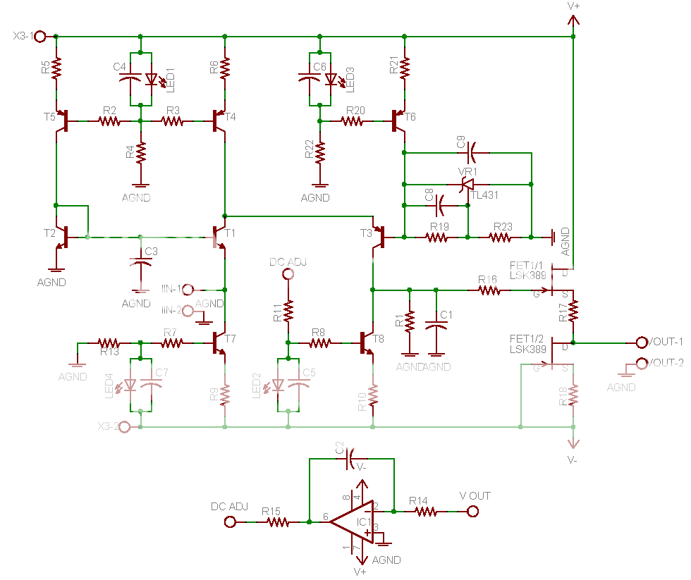
I thought I would post my schematic for a discrete I/V converter for use on the output of an audio DAC here, to see if anyone had any comments or suggestions as to how I could improve it. BJTs will most likely be 2SC2240BL/2SA970BL parts, due to their extremely high hFE which remains quite linear with regards to IC for the values of IC I am interested in, which is ~10mA, as well as the low noise and capacitance of this part. If anyone knows of any other parts I should check out instead, both smd and through hole, I would appreciate it.
I plan to pair this converter with AD1862N-J DACs, though it will work with other current out designs. I currently own four of these chips and will designing the DAC to have true differential outputs by creating an inverted digital signal with a pair of XORs after the SM5847 8x OS digital filter (I have two on the way). I really wish I could get my hands on a PMD-100 (who doesnt?), but I havnt seen any available, at least for a price that I consider reasonable. I will need to implement a bit of glue logic to allow this filter to accept input from the PCM2707 I²S output which I intend on using as my primary input for the DAC. SPDIF will probably come in the form of a CS8414, and I will use something like the Omron G6Z high frequency 75ohm relays to perform input switching.
Since it is an open loop design, PSRR is a concern, but due to the heavy use of current sources, and the folded cascode topology, I believe that with decent rail regulation and filtration, this will be a non issue. PS regulation will be either by CCS fed shunt regs, or jung style series regs.
There are some changes I am currently evaluating for this design. First is the addition of cascodes on all current sources, though this should be most beneficial for the one based around T8, but hey, cascodes are like cookies, you cant just stop at one. I am also contemplating replacing the current base biasing solutions with emitter-followers, connected for base current error correction as shown by Malcolm Hawksford in his paper "Current-Steering Transimpedance Amplifiers for High-Resolution Digital-to-Analogue Converters". I also may increase the number of poles in the low pass filter, but a 3rd order design is the highest I am considering, and I am hoping I can get away with fewer poles. Finally, I am thinking about replacing the open loop JFET buffer with a discrete opamp, since the RC low-pass filter will drastically reduce the extreme high frequency output of the DAC, which is the primary reason for the converter being open loop in the first place. If I do this, however, I would be greatly inclined to make this opamp my headphone amplifier, since I dont like the idea of using two opamps in the signal path when unneccessary. By adding a high current discrete buffer, either diamond or some MOSFET topology, after the VAS of the opamp, I could have a very nice headphone amplifier. I dont really care for the idea of having my headphone amp integrated into my DAC, and it presents some issues with how to impliment the volume control, as there really should be a buffer between the I/V resistor and volume attenuator. The only way I can think to get around this is handle the volume control similar to how Nelson Pass did it on the D1 DAC, with a relay controlled resistor ladder between the phase and antiphase signals on the output of the folded cascode transistor, which in my schematic is T3.
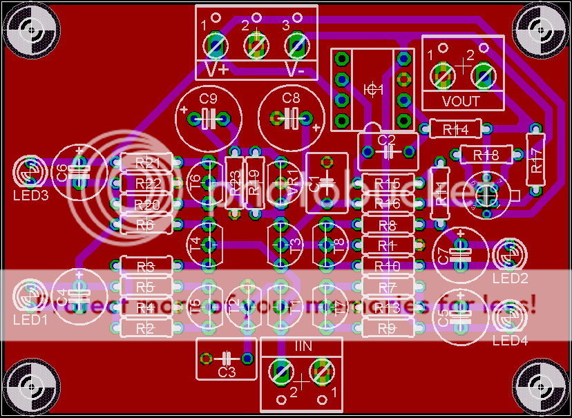
I also did a quick board layout for a single channel of this I/V. This is not actually how I intend on using it, since I plan to have four of these on the same PCB as the rest of my DAC. Also, this board shows all through hole parts, where for my final implementation, I plan to use SMD instead, at least for the resistors, which will most likely end up being 1206 package. The point of this was more to get an idea how the layout could take shape, and because I was bored.
I would appreciate any feedback people here can provide (though not globally in the I/V). For those of you who managed to stay awake to this point, thanks for putting up with my rambling.
I plan to pair this converter with AD1862N-J DACs, though it will work with other current out designs. I currently own four of these chips and will designing the DAC to have true differential outputs by creating an inverted digital signal with a pair of XORs after the SM5847 8x OS digital filter (I have two on the way). I really wish I could get my hands on a PMD-100 (who doesnt?), but I havnt seen any available, at least for a price that I consider reasonable. I will need to implement a bit of glue logic to allow this filter to accept input from the PCM2707 I²S output which I intend on using as my primary input for the DAC. SPDIF will probably come in the form of a CS8414, and I will use something like the Omron G6Z high frequency 75ohm relays to perform input switching.
Since it is an open loop design, PSRR is a concern, but due to the heavy use of current sources, and the folded cascode topology, I believe that with decent rail regulation and filtration, this will be a non issue. PS regulation will be either by CCS fed shunt regs, or jung style series regs.
There are some changes I am currently evaluating for this design. First is the addition of cascodes on all current sources, though this should be most beneficial for the one based around T8, but hey, cascodes are like cookies, you cant just stop at one. I am also contemplating replacing the current base biasing solutions with emitter-followers, connected for base current error correction as shown by Malcolm Hawksford in his paper "Current-Steering Transimpedance Amplifiers for High-Resolution Digital-to-Analogue Converters". I also may increase the number of poles in the low pass filter, but a 3rd order design is the highest I am considering, and I am hoping I can get away with fewer poles. Finally, I am thinking about replacing the open loop JFET buffer with a discrete opamp, since the RC low-pass filter will drastically reduce the extreme high frequency output of the DAC, which is the primary reason for the converter being open loop in the first place. If I do this, however, I would be greatly inclined to make this opamp my headphone amplifier, since I dont like the idea of using two opamps in the signal path when unneccessary. By adding a high current discrete buffer, either diamond or some MOSFET topology, after the VAS of the opamp, I could have a very nice headphone amplifier. I dont really care for the idea of having my headphone amp integrated into my DAC, and it presents some issues with how to impliment the volume control, as there really should be a buffer between the I/V resistor and volume attenuator. The only way I can think to get around this is handle the volume control similar to how Nelson Pass did it on the D1 DAC, with a relay controlled resistor ladder between the phase and antiphase signals on the output of the folded cascode transistor, which in my schematic is T3.
I also did a quick board layout for a single channel of this I/V. This is not actually how I intend on using it, since I plan to have four of these on the same PCB as the rest of my DAC. Also, this board shows all through hole parts, where for my final implementation, I plan to use SMD instead, at least for the resistors, which will most likely end up being 1206 package. The point of this was more to get an idea how the layout could take shape, and because I was bored.
I would appreciate any feedback people here can provide (though not globally in the I/V). For those of you who managed to stay awake to this point, thanks for putting up with my rambling.
- Status
- Not open for further replies.