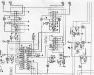
can i bypass the ic16 and 17 (NAND gate). Why the master clock is connected to pin 1 and 2 of ic 15 after connected to pin 13 for output to pin 12, it's for jitter? And enters to pin 11, out pin10, in pin 5 and out pin pin6 to the NAND gate. I don't understand this circuit. thank you! Maxpou
It looks to me like the NAND gates are performing as part of the actual d/a conversion, which is why I described it as a semi-discrete sort of mash circuit. But without specific data on the dac chip driving them, I can't really be sure. It looks to me like it has not a prayer of sounding great, no matter what you did to it, short of scrapping the whole dac section & building an entirely new one. Easier to plug it into an external dac unit, though, I think.;-)
- Status
- This old topic is closed. If you want to reopen this topic, contact a moderator using the "Report Post" button.