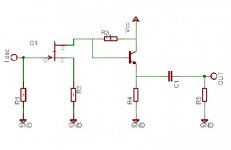
I just stumbled upon this idea of i/v stage for 1543, and I need some experienced opinion from you (anyone who build or just mind-scrolled thru all active i/v stages on this site). Its just a 'block diagram', (after R1 - its very common circuit in preamps) with huge input imp. from jfet, and very low output imp. from bjt. It has automatic bias for fet with some local feedback (and all limitations on gain and distortion?), and bjt is in just a buffer - emitter follower mode, fet voltage gain is set in coordination with R1. Which, I know that it must be small (or to be with virtual ground, like opamp i/v stage) to be harmless for 1543 performance, but how small?
Attachments
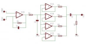
I was looking also in to this (attachment) concept, which is quasi copy of Altmann Attraction DAC output stage (which had very thundering reviews). But circuit in previous post ,I think, with its SIMPLICITY (-beauty) has more potential. Im on the EDGE of decision which circuit to use, so if anyone had stumbled upon this circuits, PLEASE help me.
Thanks.
Thanks.
Attachments
Hi Relaxin,
Seeing as you've had no response, I'll offer my opinions - but they're not worth a lot).
With the first diagram, it looks to me that R1 is used as the I/V conversion circuit, and the rest of the circuit is buffering. Is that right?
Typically (although some love them) a single resistance can lead to distortion due to loading the DAC output.
I would have thought that a common base (or common gate) amplifier layout would be a better option - although it does require a very quiet power supply.
Perhaps you should look at the Pass D1 or Jocko Homo's I/V stage?
I have only used the simple opamp as an IV stage (ala 1541 data sheet) to date, but am keen to try a discrete IV version when I get the chance.
Cheers,
Phil
Relaxin,
Phil is correct. The DAC current output stages distort when driving more than 5 ohms or so, and ideally should be driving a virtual ground. If you set your R1 to 5R so that the DAC doesn't distory then the active stage of your I/V converter would need to have a gain of ~46dB to give you decent output levels. However, getting 46dB of gain and decent distortion levels with a simple two transistor buffer is probably not a realistic expectation.
That being said, since the I/V is that simple, it will be cheap and very easy to build, so there is nothing lost in giving it a try, and the results may surprise us all. Just make sure that the power supply for the I/V is quiet, as that circuit will have very little power supply noise rejection.
I'm playing around with an active I/V stage at the moment using a mosfet in common gate configuration for the input with a second mosfet forming a folded cascode around the first one. To get the distortion levels I want I am having to run split supply rails at +/-22V, bias the the mosfets to about 2/3 - 3/4 of their max power rating, and use a power supply regulation circuit that is 10x more complex than the I/V circuit. I'll post the circuit when I have all the bugs worked out, if I ever get all the bugs worked out! I guess what I'm trying to say is that half the fun is trying out ideas to see if they work.
Cheers, Terry
Hi Terry,
That sounds interesting.
I will hopefully, one day, try a common base I/V converter (simply because I am more familiar with bipolars). But I have a few other priorities first.
I was hoping to use a fairly standard regulator (like 317) followed by a transistor bypassed TL431 as a secondary regulation stage for my circuit (although I am aware that may not be good enough).
What kind of regulation are you intending? Is it more complicated simply because its +/- 22v?
Cheers,
Phil
Thank you for posting. I unintentionally forgot about this thread, and started to design another active I/V circuits.
I don’t know why you are so much scared from loading the 1543 with couple ohm load, considering that half of the world build 1543 passive design with couple thousand ohms loads, and are very happy with the sound . The proof of distinctive transparency and realistic micro dynamics (like Lowthers
 ") ) in passive 1543 design is too evident in all of mine passive variations of 1543 basic schematics, and that’s by all means, not easy to achieve. This achievement alone was enough for me, but I become greedy
) in passive 1543 design is too evident in all of mine passive variations of 1543 basic schematics, and that’s by all means, not easy to achieve. This achievement alone was enough for me, but I become greedy  and started to look for more details, macro dynamics, 3d rendering of the sound stage and all things which you can ask from high bit (octane) DAC. (forgetting that the distinctive allure of 1543 its not in the performance and finesse, but in simplicity). And then I started to read and work on active designs. (and almost broke my brains zero-jitter clock
  with reading and browsing thru all designs on this forum).
About this circuits, on the first one I don’t think that common base circuit would be better (would be more complex, and that’s for sure), if load resistance is kept low, and that may be into a decade ohm range for smaller gain requirements from active stage, (also you are sooo much right about PSRR of this simple circuit - be aware). And second circuit, (which I choose to work with) first of all, is pretty much basic active opamp circuit, with very capable output stage (also considering Altmann opamp choice, very silent-noise--->dynamics). I now work with simple circuit containing opa2134 for I/V stage and ths4032 for buffer, but I don’t have time resources to test it, instead I will directly design PCB and build it like a quasi final circuit and then compare it with passive circuit, and with discrete circuit (on proto board) if I have time, and hopefully I will post here my impressions.
I don’t know why you are so much scared from loading the 1543 with couple ohm load, considering that half of the world build 1543 passive design with couple thousand ohms loads, and are very happy with the sound
. The proof of distinctive transparency and realistic micro dynamics (like Lowthers ) in passive 1543 design is too evident in all of mine passive variations of 1543 basic schematics, and that’s by all means, not easy to achieve. This achievement alone was enough for me, but I become greedy and started to look for more details, macro dynamics, 3d rendering of the sound stage and all things which you can ask from high bit (octane) DAC. (forgetting that the distinctive allure of 1543 its not in the performance and finesse, but in simplicity). And then I started to read and work on active designs. (and almost broke my brains zero-jitter clock with reading and browsing thru all designs on this forum). About this circuits, on the first one I don’t think that common base circuit would be better (would be more complex, and that’s for sure), if load resistance is kept low, and that may be into a decade ohm range for smaller gain requirements from active stage, (also you are sooo much right about PSRR of this simple circuit - be aware). And second circuit, (which I choose to work with) first of all, is pretty much basic active opamp circuit, with very capable output stage (also considering Altmann opamp choice, very silent-noise--->dynamics). I now work with simple circuit containing opa2134 for I/V stage and ths4032 for buffer, but I don’t have time resources to test it, instead I will directly design PCB and build it like a quasi final circuit and then compare it with passive circuit, and with discrete circuit (on proto board) if I have time, and hopefully I will post here my impressions.
Looking at the second schematic, its very similar to what I am currently using, with a buffer made of four op amps in parallel.
I don't bother with a buffer, and it works fine (I do have a discrete buffer in the preamp thats serves the same purpose).
This arrangement works fine for me, and allows me to play with different opamps.
Currently, I use a single LM4562 opamp for both channels and it sounds great.
For I/V conversion, make sure the opamp doing the conversion has a high GBP|slew rate. I originally used a BB2132 for this purpose (I had used it for something else and loved the sound) but tried several other types and discovered far more detail. I used an LT device for a while (can't remember the name, but it was about 16MHz) and then went to an LM 6172 (incredibly fast opamp!) and then settled on the LM4562 (which I think is about 50MHz.
I think I'd use a single opamp for the buffering stage - so you're not stuck with the quad package suggested in the design, and you can experiment (like above).
I'm really happy with my opamp I/V conversion. It was a great starting point, but do want to move onto a discrete version.
Originally posted by philpoole
I will hopefully, one day, try a common base I/V converter (simply because I am more familiar with bipolars). But I have a few other priorities first.
I was hoping to use a fairly standard regulator (like 317) followed by a transistor bypassed TL431 as a secondary regulation stage for my circuit (although I am aware that may not be good enough).
What kind of regulation are you intending? Is it more complicated simply because its +/- 22v?
I've worked with the regulation config of 317 / 431 you mention, and it would very likely meet the noise level requirements for the I/V stage I'm trying to get working. The +/-22V isn't so hard to meet with standard regulation methods, but I decided to go for the so-called "moon shot" and I've finally got working a circuit that uses a CRC pi filter, followed by an LM317 reg, but after that I've got a discrete built shunt regulator circuit that gives ~120dB noise rejection from 1kHz up to ~4MHz tackling the bandwidth where the 317 doesn't work so well. I took the idea from one of the John Curl threads and put my own touches to it. Along the lines of a CCS feeding a voltage reference for a higher current CCS that feeds the load and a shunt transistor whose voltage reference is CCS biased. Damn touchy thing to get working stable, but once stable the performance is phenomenal.
I'm mainly going to all this trouble because I want to see if there is a real benefit to keeping the I/V stage as simple as possible. It has no CCS's, current mirrors, feedback or other means of achieving linearity. It relies solely on optimizing the voltage and bias levels across the FET's and the cascode.
I finally got the regulation circuit and the I/V stage to be stable when working together, and now I need to connect it all to the DAC output, and see what new surprises that turns up. After eight months trying to get this thing working properly, what is another month or two of troubleshooting.
Cheers, Terry
Hi relaxin,
Sorry, I probably wasn't paying much attention. I was mainly referring to the schematic.
With regard to testing. I built mine without testing. I don't think you can do too much damage if its not quite right (mine wasn't working on one channel to start with). 1543s are cheap if it does go wrong.
Hi Metalman,
The regulation sounds like a fairly major project in its own right - but its probably the best part of the system to put such hefty regulation. Sounds like a lot of current sources!
Glad to hear my intial plan should suffice. I would also have two current sources (one to the collector, one to the emitter), so it should be quite fun to build - if I ever get round to it.
How do you find a discrete stage performs in comparison to the standard opamp equivalent (or passive IV for that matter)?
Cheers,
Phil
I have a passive/active output stage in my mind. It has the I/V resistor on the secondary of the transformer. The I/V resistor is formed by the input impedance of the upper and lower cathodes. This resistance is transformed back to the primary with the turns ratio squared, so the DAC can see a very low load (I designed it for the TDA1541A). The tube output is the well-known SRPP circuit built with E88CC/6DJ8, and the cathodes are driven in perfect push-pull. The quiscent sink current of the DAC chip is not indicated on the diagram (half-scale, 7FFF digital input, 0 V audio output voltage.
I haven't built this circuit yet, I am just looking for a suitable transformer. Maybe a larger turns ratio will prove to be better, and perhaps I have to put some parallel load resistance to the secondary windings.
I haven't built this circuit yet, I am just looking for a suitable transformer. Maybe a larger turns ratio will prove to be better, and perhaps I have to put some parallel load resistance to the secondary windings.
Attachments
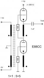
I forgot to mention that I intend to use two TDA1541As driven with complementary offset binary data, thus yielding push-pull output currents. I hope this arrangement will improve linearity. The DC resistance of the primary and the transformed DC resistance of the secondary windings have to be calculated in, their sum should be less than 5 ohms seen by one DAC output. I am considering a Lundahl LL1678 transformer, originally recommended for MC pickups, connected at 1:16. The primary resistance is 2.25 ohms, it seems sufficiently low for the purpose.
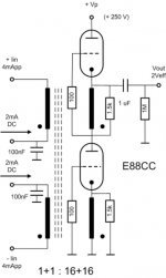
The transformer/tube output stage is singing finally! I connected it to the output of the TDA1541A non-oversampling DAC that is built in my Marantz CD-74 on a piggyback board. Previously I used OPA627As without analog filtering. I am happy with the experimantal tube unit because there is no hum or noise at all. After a quick listening the main difference is somewhat more depth of stage, but I need to listen more to fully explore the difference. I intend to install a switch in the player to enable quick A/B testing.
Currently I use one DAC that drives one primary only, not two DACs in differential mode, driving the two primaries in push-pull as planned. Now the bias current of 2 mA flows through the primary (one end grounded, other end to the DAC). This may push the operating point of the transformer up the hysteresis curve. In push-pull mode the bias currents will cancel just like in a push-pull power amplifier.
Currently I use one DAC that drives one primary only, not two DACs in differential mode, driving the two primaries in push-pull as planned. Now the bias current of 2 mA flows through the primary (one end grounded, other end to the DAC). This may push the operating point of the transformer up the hysteresis curve. In push-pull mode the bias currents will cancel just like in a push-pull power amplifier.
- Status
- This old topic is closed. If you want to reopen this topic, contact a moderator using the "Report Post" button.
- Home
- Source & Line
- Digital Source
- Passive-Active I/V stage