This is my first time doing something just from the schematics. Unfortunately I don't have no other than basic knowledge in electronics so it took me days to figure this out alone...
I wonder if I have done it correctly. I am opened to all suggestions.
Thanks!
I wonder if I have done it correctly. I am opened to all suggestions.
Thanks!
Attachments
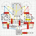
Schematic+debuged version
Here it comes!!!")
lucpes said:If you attach the schematic you might get a reply
Here it comes!!!
Attachments
Hi Bassivus,
Looking briefly at it, it looks good.
Glad you're thinking about star earth.
I knocked up a kwak clock quite roughly recently and started looking at the power rails with a scope to see the effects of ground bounce and ended up with nearly every component leg straight to the star ground.
(eg, r2, x1, c6 r1, r12 would each have a wire from the ground leg straight to the ground star point).
Also, it might help to have capacitance (at least c4 and c15) placed closer to the comparator, if you can.
Hope this helps, but what you have will probably work well (I've built a few before without any care to layout and they work quite well)
Cheers,
Phil
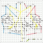
 like I was suggested, and this is the new version I came up with:
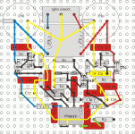
Hi, How fast is the clock running if it is > 10MHz then the star earth topology you are using is probably not the most appropriate as the signal will follow is the field between the out bound path and the return path. In this situation a ground grid is usually better (basically this just means connect the grounds together in as many locations as possible to reduce the return ground impedance as far as possible and provide the sortest return path possible)- or if possible the logical extension for this a ground plane. At the very least I would connect from R12 accross to the ground on the driver chip so there is a return path for the curent from the oscillator that does not have to try to flow though the PSU ground.
The other thing I am concerned about is you have no ground take off for the signal leaving the PCB there should be a ground terminal next to the output signal terminal this should return to the ground on the driver chip not the star (In your case this is the centre point of the two decoupling caps C15 and C4). Stars do not work well at high frequencies you should think of the signal following in the field between the ground return and the signal trace and try to make the field area as small as possible.
Regards,
Andrew
Hello,
Thanks very much for the advice! Last time when I have posted I almost have put to the question the situation with R12 and C4/C15 ground, that you just have explained! Great!
If I have understood correctly it should be OK/good to connect R12 GND to the center point of ground between C4/C15 and than jumper/connect to PSU ground center?
Regards, Ivica
Hi,
It is looking better but I would try to get a connection from Pin 6 over to R12 as well so there is a diret return path for the signal from the Crystal. As noted in the last post if you can get a board with a ground layer on one side this would be better, however I realise that for home build that may be quite difficult.
Also dont forget to take the ground to a terminal from the driver chip to go out with the signal to your main board and use coaxial cable to connect it.
Regards,
Andrew
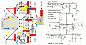
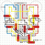
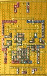
NEW GROUND PLANE DESIGN
Hi,
I finally got one of the proto boards with the lines connected and changed the design accordingly. Now I got big ground plane like suggested and added the missing GND out, Andrew pointed . Actually, before, I was confused weather there should be a connection between CDP GND and KC GND (not to mention "in/out" gnd). I now that the drawing looks unclear and too much colorful but I had to do it this way not to mess up the lines... Note that this time the view is from under the board. Yellow doted lines are jumpers on the upper side. Colored rectangles are brakes in continuity of board ground lines.
Once again thanks everybody for help, and special thanks to Andrew!
Regards, Ivica
Hi,
I finally got one of the proto boards with the lines connected and changed the design accordingly. Now I got big ground plane like suggested and added the missing GND out, Andrew pointed . Actually, before, I was confused weather there should be a connection between CDP GND and KC GND (not to mention "in/out" gnd). I now that the drawing looks unclear and too much colorful but I had to do it this way not to mess up the lines... Note that this time the view is from under the board. Yellow doted lines are jumpers on the upper side. Colored rectangles are brakes in continuity of board ground lines.
Once again thanks everybody for help, and special thanks to Andrew!
Regards, Ivica
Attachments
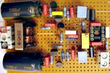
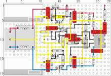
Bassivus said:I have finished the job and this is how it looks.
I have tested it for the supply only(like in the pic.) without cristal and comparator on and it works fine...
Ivica
A ground plane solution would have been to cover the top of the board with copper adhesive tape and cut square holes through that where the components fit in...
Hi, Very neat looking design. I hope it works well for you. Whilst a ground plane probably would be better I think you will get good performance from your current implementation.
Do you have any way to test it before wiring it up - ie. an oscilloscope? As this would help to confirm performance and minimise the chance of damage to the product you are going to put it in.
Regards,
Andrew
Do you have any way to test it before wiring it up - ie. an oscilloscope? As this would help to confirm performance and minimise the chance of damage to the product you are going to put it in.
Regards,
Andrew
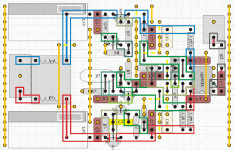
Hello,
I thought I made it (almost) a ground plane design. It is not obvious from the top view however. Maybe the pic from uder side is more clear. I painted in yellow the area covering ground.
Ivica
I thought I made it (almost) a ground plane design. It is not obvious from the top view however. Maybe the pic from uder side is more clear. I painted in yellow the area covering ground.
I plan to visit some guys with the oscilloscope to tune it next week.gfiandy said:...Do you have any way to test it before wiring it up - ie. an oscilloscope? As this would help to confirm performance and minimise the chance of damage to the product you are going to put it in...
Ivica
Attachments
I think the problem here is somantics. What you have done is a ground fill, which is the best that can be achieved on a one sided PCB. What is being suggested is that a two sided board with solid copper on one side connected to ground would work better. Whilst this is true I think you have done the best that you can with the solution you have and in the end electronics is always a set of compromises.
I hope it all goes well when you test it. be sure to use a very short ground connection on the scope. Even the little bit of wire with a clip on the end that come on most probes is far too long for signals above 10MHz. The best solution is to solder a peice of thin solid copper wire to the ground as close as possible to the signal you want to measure then wrap it round the exposed ground on the tip of the probe.
You can get some idea of what is going on with the clip first then try with a short soldered lead afterwards, you will be amazed by how the signal changes an how much more of the actual signal you can see.
Regards,
Andrew
- Status
- This old topic is closed. If you want to reopen this topic, contact a moderator using the "Report Post" button.
- Home
- Source & Line
- Digital Source
- Could somone please check my KC Protoboard?