Since that other thread disintegrated, I'll post my stuff here. Here is a schematic and layout for a 24-bit, 96kHz, stereo DAC. You should be able to build this for less than $300. The board is run from a +/-10V supply fed in through the molex connector at the top. The 16-gauge output pads are, from top to bottom, R-, R+, L+, L-. Coupling capacitors and output resistors are needed, but I left them off so you can make them to your taste. Note also that I have neglected all inputs. Hook them up to pins 4 and 5 on the CS8420 as you wish, and place them in the vast empty space on the board's periphery.
Many features are left as an exercise for the reader. You could make this DAC better, and you could make it cheaper. Please post any modifications you make here!
NB: this design is untested, as I have not built it and in fact have no plans to build it. I drew it only because I was intrigued by peranders' idea of a DAC costing less than $300.
schematic
Gerber files
An externally hosted image should be here but it was not working when we last tested it.
jwb said:Since that other thread disintegrated
I surely agree!
Looks nice, your pcb, but what about analog and digital groundplanes? Crystal claims that this is really important in order to get high S/N. The thing that worries me the most is in fact EMI. These nasty waves seems to wander through my LF-section despite the fact of having separate groundplanes and separate power supplies.
Your "minimalistic" solution can be a good start of a decent DAC.
What is a bad DAC?
What is a fair DAC and what is an excellent DAC?
Some thinks that only Burr-Brown fits but I have noticed that Crystal and AKM are very common in professional gear, so they can't be that bad. After all, many CD's are created with Crystal and AKM in the signal chain. Just a thought.
300 USD is very realistic if you are lucky, home made pcb's, cheap case, free samples, junkbox full of junk etc.
Well there is no need for I/V conversion with the Cs43122 since it outputs voltage. a buffer should suffice? maybe even transformer coupling?
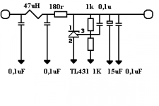
The LT1962 seems quite hard to find what about somthing simpler like a TL431 ?
In my opinion the PCB should be made to be easily made at home that means no traces thinner than 1mm not to many vias. and only 2sides.
separate groundplanes should not be so hard to make.
Is the AKM dac voltage out? than maybe some form of adaptercard can be used for the dac to make it mor universal?
just my 2c
/micke
btw...is this still peranders show or is it a diyaudio.com project now?
Attachments
Jocko Homo said:I couldn't open the Gerbers either. Is there an aperature file that we are missing?
The file is for Gerber RS274X. The apertures are embedded. I can view them with gerbv (linux) and with Viewmate (windows). The drill file is missing. I'll add it when I get back to that computer.
I've seen similar I/V schematics up here before. I suggest that you might want to test it first, as some have distortion numbers higher than you might want to accept.[/B]
This isn't an I/V scheme, it's just a buffer and line driver. The output from the DAC is voltage, but I wouldn't want to drive a cable with it. In the world of source followers, I think this one is pretty common.
Re: Re: Cheap 24/96 DAC with CS43122
You can slot the groud plane around the output buffer and the topmost regulator, but you must leave it connected beneath the DAC. The problem will be that two +10V power traces will cross this slot, and their return path to ground will be directly beneath the DAC. That would be worse, I suspect.
The solution is probably to bring in +10/GND/-10 on the top connector, and add a connector on the bottom for +10/GND. Cut the power traces that cross the slot.
I think the key here is not to separate the ground planes, but to consider all the return paths for every signal you route. In this layout, I made certain there are no high-speed digital signals with return paths through the analog section. In fact all the digital crap is confined to a small area in the center of the board. The +5V rails are all decoupled with capacitors practically atop the power pin, and I have provided a nice fat via to ground from each ground pin. The +10V rail feeds the regulators via ferrite beads (L1, L2, and L3), so I expect the +10V rail to be quiet.
As I said, this is a simple DAC with embellishments left to the reader. A split ground plane and independent supplies with separate transformers would be one of those embellishments.
peranders said:Looks nice, your pcb, but what about analog and digital groundplanes?
You can slot the groud plane around the output buffer and the topmost regulator, but you must leave it connected beneath the DAC. The problem will be that two +10V power traces will cross this slot, and their return path to ground will be directly beneath the DAC. That would be worse, I suspect.
The solution is probably to bring in +10/GND/-10 on the top connector, and add a connector on the bottom for +10/GND. Cut the power traces that cross the slot.
Crystal claims that this is really important in order to get high S/N. The thing that worries me the most is in fact EMI. These nasty waves seems to wander through my LF-section despite the fact of having separate groundplanes and separate power supplies.
I think the key here is not to separate the ground planes, but to consider all the return paths for every signal you route. In this layout, I made certain there are no high-speed digital signals with return paths through the analog section. In fact all the digital crap is confined to a small area in the center of the board. The +5V rails are all decoupled with capacitors practically atop the power pin, and I have provided a nice fat via to ground from each ground pin. The +10V rail feeds the regulators via ferrite beads (L1, L2, and L3), so I expect the +10V rail to be quiet.
As I said, this is a simple DAC with embellishments left to the reader. A split ground plane and independent supplies with separate transformers would be one of those embellishments.
hifi said:In my opinion the PCB should be made to be easily made at home that means no traces thinner than 1mm not to many vias. and only 2sides.
You can't have these constraints and work with these parts. The pads on SOIC are .5mm wide. You can't route to them with 1mm traces. You'll notice I had to route traces beneath the SOICs. There isn't enough room for four 1mm traces in there.
As for vias, they are critical to performance. Every IC ground pin must have a low impedance path to the ground plane. Every decoupling capacitor, or group of capacitors, should have a via to ground as well. I think I kept vias to a minimum here. There are no vias on signal or power traces, only vias to ground, and I have used only .050", .040", and .020" drills.
btw...is this still peranders show or is it a diyaudio.com project now?
I told you. We're an anarcho-syndicalist commune. We take it in turns to act as a sort of executive officer for the week. But all the decisions of that officer have to be ratified at a special biweekly meeting. By a simple majority in the case of purely internal affairs, but by a two-thirds majority in the case of more ...
I have downloaded viewmate now so I will take a look att the layout now.
Ofcorse you can make a card like that at home i simply meant that wider traces and as few vias as possible would make it simpler to make it but i have mannaged to etch for ssop capsules att home but maybe not everybody that wants to build the dac can do so.
/micke
Ofcorse you can make a card like that at home i simply meant that wider traces and as few vias as possible would make it simpler to make it but i have mannaged to etch for ssop capsules att home but maybe not everybody that wants to build the dac can do so.
/micke
I agree, single groundplane will usually outperform split planes in terms of EMI. Any potential differences across the split will cause the two ground planes to act like an antenna, transmitting and receiving EMI. Proper supply decoupling and careful control of ground return paths is the way to take care of noise problems on a mixed signal board. By ground return paths, I mean both signal return paths and supply return paths.
Decoupling can be greatly assisted with the use of ferrite beads and resistors to block high frequencies from wandering around the board. Tight local supply loops through the shortest path around each IC are important too. This minimizes series inductance in the path through the decoupling cap. Using SMT ceramic chip caps on the backside of the board, directly beneath each chip is a good method. I've also considered that using crappy electrolytics to decouple digital ICs might be a good thing, since their higher ESR may have a damping effect on power rail fluctuations... provided, of course that you have appropriate low-impedance decoupling caps in place to absorb HF stuff. I haven't personally done any measurements on this particular idea, but it seems reasonable to me.
Anyway, my point is that there are better ways to take care of noise problems on a PCB than splitting the ground plane. Sometimes, only a partial slit in the groundplane is needed to isolate immediately adjacent sections, and I feel this is preferable to a total split. Lastly, a chip generally needs continuous ground plane beneath it. A ground plane split beneath an IC can really mess it up if you're not careful. As usual, there are a few odd exceptions, but AFAIK, DACs are happier living on top of continuous ground plane.
As for the PCB, SMT will demand the use of fine features on the copper. It is not too hard to do at home... I rarely bother etching my own boards any more, given how inexpensive commercial services have become, but with some basic photo-resist methods, I was easily able to achieve the necessary resolution to do fine-pitch SMT stuff. Plated vias are really nice, but not too many people can do that at home, so you can just put a solder pad on either side of a hole and connect through with a short bit of component lead or something. Anyway, maybe you can see why I have a preference for commercially produced boards. So much less work, IMHO the board easily pays for itself in reduced hassle and superior end product.
hifi - oh you posted while I was composing...
I guess you're right, not everyone can build a board like this too easily. Again, commercial board services to the rescue. And that's what's so great about this forum... group buys!!! If the design is a good one, chances are people can get together and split the cost of manufacture, which should make it easier to swallow for those on a tight budget.
Personally, I consider the PCB a <i>major</i> component in my projects, and allocate budget accordingly. I don't understand people who skimp out on the board, but go nuts buying expensive ICs and fancy resistors.
http://www.diyaudio.com/forums/showthread.php?threadid=3282&perpage=20&highlight=kasra&pagenumber=6
I vould vote for this inputstege...or is the AD8561 a bitch to comeby??
/micke
I vould vote for this inputstege...or is the AD8561 a bitch to comeby??
/micke
")
Re: Re: Re: Cheap 24/96 DAC with CS43122
Are you really sure about this?
This emphasizes ALL chip manufactures very cleary. They even suggest multi-layer board in order to squeeze everything out from chip in forms of performance.
I haven't got the opportunity to test how much difference it makes, but somehow I think this might be very true.
My goal in my DAC is to really "get out" everything from the chip. I don't want any colouration at all and the filters should be very low noise ones.
To do a 100 dB circuit isn't so hard. 110 dB needs care and 122 dB is extremly difficult if we talk line level signals. As I see it, the RF-emission is the crook. Even the oriention of the parts are (can be) essential here.
jwb said:I think the key here is not to separate the ground planes...
Are you really sure about this?
This emphasizes ALL chip manufactures very cleary. They even suggest multi-layer board in order to squeeze everything out from chip in forms of performance.
I haven't got the opportunity to test how much difference it makes, but somehow I think this might be very true.
My goal in my DAC is to really "get out" everything from the chip. I don't want any colouration at all and the filters should be very low noise ones.
To do a 100 dB circuit isn't so hard. 110 dB needs care and 122 dB is extremly difficult if we talk line level signals. As I see it, the RF-emission is the crook. Even the oriention of the parts are (can be) essential here.
hifi said:btw...is this still peranders show or is it a diyaudio.com project now?
This isn't my show in that respect but I will contribute here if you think I have something to say.
Remember though that my show is also totally free except for the gerber files. Anyone who wants to make his own pcb's is welcome to do that, but the traces will be 15 mil many of them and if I choose AKM it will be chip with 0.65 mm between the pins.
- Status
- This old topic is closed. If you want to reopen this topic, contact a moderator using the "Report Post" button.
- Home
- Source & Line
- Digital Source
- Cheap 24/96 DAC with CS43122