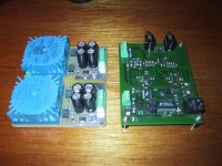
unfortunately no schematic in electronic form.. the i/v is simply this (from ad1853 datasheet): (implemented to house 4xsoic + 2xdip opa627).. the ic chain is as follows:
ua9637 RS422 differential receiver
dir1703
ad1853
6x opa627
a tl7733 is used to generate the reset signal and 2xadp3303-5 generate the digital and analog 5v for the AD. An additional 780-05 to provide for the UA9637 and an 78033 for the DIR..
ua9637 RS422 differential receiver
dir1703
ad1853
6x opa627
a tl7733 is used to generate the reset signal and 2xadp3303-5 generate the digital and analog 5v for the AD. An additional 780-05 to provide for the UA9637 and an 78033 for the DIR..
Attachments
Hi,
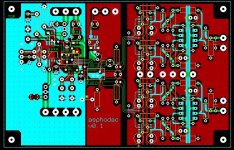
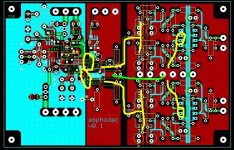
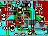
Its not a bad layout.
I am assuming you have a power supply board somewhere and are connecting to the converter by connectors/wires?
I would recommend that you integrate the power supply onto the converter board. Remote PSUs (unless you are using a switchmode) are usually a waste of time and offer negligible performance gains in terms of both noise and distortion. Often this remote power approach actually introduces more noise due to the inherent cable and trace inductances.
Also I see that you are using separate ground planes for the different sections of the board. This is also often done to reduce digital noise from entering the analog circuitry, however many semiconductor manufacturers (and off memory Analog Devices have a very good app note on this) recommend a continuous ground plane. In my experience (power electronics, RF, digital audio and DSP background) this bears true.
Kirchoff's laws state that current flows in loops, however unless you can see the actual path taken by electrons it is better to let them decide where is the path of least inductance.
For instance in your connections between the converter and your analog stages you are using two separate planes. Yet you have the current output traces crossing this gap.
This would force the return current to flow from your analog stage, back to your powersupply (near the other supplies) and back to the converter via the relevant ground connection. Its a big loop. And loops radiate noise as well as receive it.
And you have big cuts in your planes... introducing more antenna/loops inductance effects.
Also of note is that if you mount the PSUs on the board near the relevant sections and run the secondary AC to them, you only have one frequency of noise to worry about (50/60Hz) local harmonic generation will be confined to the local loops (small) and thus this approach should be of lower noise.
And dont put any cuts in your plane across ANY clock signal... 24MHz digital audio clocks have odd harmonics extending into GHz and this will definitely be picked up by the rest of the board's loops...
Hope this helps!
Apollyon25
Hi costiss,
A good layout indeed. I like those I2S bus, short and direct.
I also agree with apollyon25 about continuous ground plane. I suggest the DAC analog section and the post filter section sharing common ground plane.
Attached my AD1853 layout.
A good layout indeed. I like those I2S bus, short and direct.
I also agree with apollyon25 about continuous ground plane. I suggest the DAC analog section and the post filter section sharing common ground plane.
Attached my AD1853 layout.
Attachments
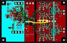
forgot to mention that: the i/v analog plane will be connected to the dac analog with some heavy gauge short cable.. its just that the space didnt allow for a single thick track to connect them both.. so its done with a cable soldered between them.. so is the case with the plane in front of the iv's.. theres actually sth like a star ground for the analog part, right where the guards connect.. regulation for the digital part and the dac analog supply are on board.. and i have provided for decoupling caps for each chip.. so i dont think there wikll be loops.. the only connection between the grounds of the supplies is on board, so no loops.. look, thats the cable connections..
Attachments
Hi Costiss,
Your DAC board looks great. I also built a AD1853 DAC based on Analog Devices Eval board. I used a CS8414 decoder and op2604 opamps. I also designed a small power supply to use with it, and used a Digital Rheostat to control the output volume on board. It's a great sounding DAC. If you have any problems getting it working let me know. It's been a while since a built mine so I may have to refresh my memory but I'd be glad to help. Here's a pic.
Best regards,
Al
Attachments
Banned
Joined 2002
AAK said:Hi Costiss,
Your DAC board looks great. I also built a AD1853 DAC based on Analog Devices Eval board. I used a CS8414 decoder and op2604 opamps. I also designed a small power supply to use with it, and used a Digital Rheostat to control the output volume on board. It's a great sounding DAC. If you have any problems getting it working let me know. It's been a while since a built mine so I may have to refresh my memory but I'd be glad to help. Here's a pic.
Best regards,
Al
Got any pictures looking straight down at the boards ?
I like the psu boards Good job..

Costiss,
I understand what you are trying to do, as I have designed a commercial D/A converter unit for a prominent audio company.
However you have missed the point of the whole loop conversation.
A cable as you have shown may work, but it is far from optimal.
You have to realise that there are lots of current loops in a circuit.
Decoupling capacitors really only supply a minimal amount of transient response energy to a device and usually perform the removal of HF noise currents from the device by shunting them to ground. Local reservoir capacitors should be used to supply the transient device currents (I use a bead inductor, an electrolytic capacitor, and a small ceramic decoupling capacitor mounted AT the supply pins).
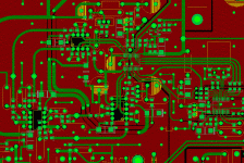
Have a look at the attached pic. I have drawn on it to illustrate the problem areas. Also as far as I can tell there is no connection between the I/V input side and I/V output side of the ground plane... where are the currents going to get to ground?
Particularly important are the current outputs from the DAC. Have a look at the loop between the yellow scribbles and the green 'gnd cable' scribble... thats a big loop! I am sure it will pick up your EMI from the clocks nicely!
Similarly on the input to the converter.
Basically as a rule I try to route EVERYTHING on the top layer, and leave the bottom layer ENTIRELY ground. If there are any cuts for required tracks - move them away from critical areas.
Inputs to opamps are high impedance so they pick up LOTS of noise.
If you are making this board yourself pay (and dont have through hole plating) ensure you think about how you are actually going to solder the bits BOTH SIDES.
If you want to discuss this further I leave msn messenger running while I am at work (and often at home too)
apollyon25 at hotmail dot com
hope this helps
apollyon25
I understand what you are trying to do, as I have designed a commercial D/A converter unit for a prominent audio company.
However you have missed the point of the whole loop conversation.
A cable as you have shown may work, but it is far from optimal.
You have to realise that there are lots of current loops in a circuit.
Decoupling capacitors really only supply a minimal amount of transient response energy to a device and usually perform the removal of HF noise currents from the device by shunting them to ground. Local reservoir capacitors should be used to supply the transient device currents (I use a bead inductor, an electrolytic capacitor, and a small ceramic decoupling capacitor mounted AT the supply pins).
Have a look at the attached pic. I have drawn on it to illustrate the problem areas. Also as far as I can tell there is no connection between the I/V input side and I/V output side of the ground plane... where are the currents going to get to ground?
Particularly important are the current outputs from the DAC. Have a look at the loop between the yellow scribbles and the green 'gnd cable' scribble... thats a big loop! I am sure it will pick up your EMI from the clocks nicely!
Similarly on the input to the converter.
Basically as a rule I try to route EVERYTHING on the top layer, and leave the bottom layer ENTIRELY ground. If there are any cuts for required tracks - move them away from critical areas.
Inputs to opamps are high impedance so they pick up LOTS of noise.
If you are making this board yourself pay (and dont have through hole plating) ensure you think about how you are actually going to solder the bits BOTH SIDES.
If you want to discuss this further I leave msn messenger running while I am at work (and often at home too)
apollyon25 at hotmail dot com
hope this helps
apollyon25
Attachments
Costiss,
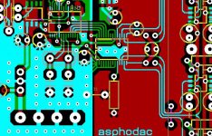
The analog side is now MUCH better.
As for how to connect the two ground planes. I am not sure. I do not know which package you have used for schematic entry and PCB design. It doesnt look like anything I have used before (Protel and PADS).
The way I have done split planes that are connected is to insert cuts into the plane with "layer specific keepouts". The polygon pour then fills around these. NOTE that the cuts I am referring insert a physical separation between sections of the circuit.
How this is done depends entirely on your software and how it manages its design rules and connectivity (net) information.
Typically though the two planes are joined at the DAC converter device as there is usually an internal connection of some form there anyway. AD have a couple of 'design guide' books that are taken from app notes about correct grounding of ADC/DAC systems for improved noise performance.
Remember when making cuts in the plane that at DC/LF the return currents will flow in the path of least resistance, but at higher frequencies the currents follow the path of least impedance. At HF this usually means on the ground plane DIRECTLY UNDER THE TRACE OF INTEREST.
Eg. A clock signal for a DA Converter goes from the clock to the device, then back via the ground to the clock. The electron flow is back to the clock ground, on the ground plane, DIRECTLY UNDER the trace to the converter. This is the path of least impedance (least inductance usually). By making the return current deviate from this ideal path it introduces a loop area (and loops are very good antennas!).
What this means essentially is that under every trace there should be a ground plane.
Basically go through your circuit and identify the sorts of signals you have... fast clocks, Hi Z opamp inputs, noisy power, clean power, etc and separate them (except where they connect obviously). Fix what you can, i.e. make all supplies clean, insert beads, reservior caps, and decoupling caps on all devices.
Isolate the rest.
Anyway - Enough wisdom emparted this email...
apollyon25
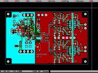
Costiss,
Better!
One other thing... especially if you are going to start actually manufacturing these.
Dont put vias in/on surface mount pads... it changes the thermal load during reflow and you may have reliability problems.
Not an issue if you are just making one... but its a bad habit to get into. I allow 25 thou from edge of pad to edge of the pad of the via, and I also try to avoid placing vias under SMT components.
The latter isnt as critical and I just avoid it from a 'best practice' point of view!
Good luck with it! I hope it sounds brilliant!
(like mine... hehee)
apollyon25
- Status
- This old topic is closed. If you want to reopen this topic, contact a moderator using the "Report Post" button.
- Home
- Source & Line
- Digital Source
- my ad1853 layout.. thoughts?