Hi I am looking for a good non onversampled DAC using the CS8414 reciever and the Analog Devices AD1865 DAC. I have searched and and found a few designs, but most have a transforemer or tube on the output....I am looking for something ultra simple. I've done quite a few DIY designs but this will be my first DAC.
Thanks.
Thanks.
Extreme Boky
If CS8414+AD1865 is used and i want to use groundplane, should DGND&AGND on CS-chip be togheter with DGND on AD-chip forming a "digital groundplane" and AGND on AD-chip forming "analog groundplane" togheter with the following stage?
In This layout he has no groundplane but DGND is tied with DGNG and AGND with AGND
thanks
tobias_svensk said:
Tobias (notice I spelled it right this time)...that looks like a fairly reasonable design, anyone got a PCB for something like this, or up to designing one. I've got all the parts I need, just noe time right now to work on a PCB design. I'd much rather not use the AD1865 built in opamps but instead go with something like tobias suggests....granted for the price of the OPA627 I could probably go with tubes...any advantages to this?
If CS8414+AD1865 is used and i want to use groundplane, should DGND&AGND on CS-chip be together with DGND on AD-chip forming a "digital groundplane" and AGND on AD-chip forming "analog groundplane" together with the following stage?
Yes, you are right. Bigger part of your ground plane on PCB1 should be DGND plane covering the whole CS chip and 1/2 of AD chip(s). The rest (smaller part) should be your AGND covering analogue sections / parts of AD chip(s). They should be connected together at only one point via single wire link. No need for ferrite beads here.
There should be a separate PCB - I'll call it PCB2, for balanced analog stage with its own ground plane. Notice that you could feed only Iout+ and Iout- (per each channel) from your PCB1 to PCB2 via short solid core wire links with no ground links between two boards here! The AGND of PCB1 and ground of PCB2 should be linked at the power supply board only, as design suggests, through short - very low resistance copper ribbons and star ground point on power supply PCB.
Design is for balanced Iout to balanced Vout (XLR).
Extreme_Boky
I am also using the opa627 with this dac utilizing the internal Rf. The ground is as Extreme_boke described. The opa627 output through Evox MKP caps. Sounds very detailed BUT the midrange is thin. Bypass caps are WIMA MKS and ELNA Duorex II 10uF.
The AD844 sound thicker BUT its treble is not as good as opa627. Currently I can�ft think of any solutions.
Any recommendations will be much appreciated
The AD844 sound thicker BUT its treble is not as good as opa627. Currently I can�ft think of any solutions.
Any recommendations will be much appreciated
I am not 100% sure if you are using Iout or Vout?
AD844 and OPA627 are very different IC's.
Vout - I would try AD826 or OP275. Midrange is OP275's middle name.
Iout - stick with OPA627 (ot try AD8065...)
The "problem" you described is the reason why people try to avoid IC stages in DAC designs... You have to learn to leave with compromises if you opt for IC stage.
Regards,
Extreme_Boky
Hi Extreme_boky
Thanks for your comments. I am using Iout with OPA627BP and the internal feedback resistor (about more than 3Kohm), no analog filtering, no buffer.
I have tried a first order filter with one WIMA FKP in parallel with Rf: with 2.2nF the DAC sounded dull (treble loss???); with 1nF the lower treble jumped out uncontrollable. So I remove the filter cap and leave the raw signal.
Looking at the I/V schematic someone posted above, the feedback R is much lower than the one insider the dac chip. But that guy uses a buffer (2N2222). Are there any benefits in doing this?
You should use oscilloscope and check the frequency response for different filters and R / C values. Also, you should load your output stage while doing this!
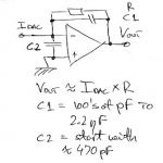
Vout max. can be calculated very simply in your case because you use extremely high impedance / low input bias current / low offset IC. (even better for I to V is AD8065!).
C1 and C2 can be determined by experiment while using oscilloscope and CD with a frequency sweep. Try not to use C2 if you don’t have to…
Buffering is good - but it is also another gain stage (A=1) that influences the original sound. You should not need buffer with your choice of I to V, unless you are driving difficult load.
Try using AD844 the way Pedja described in his TDA1541 DAC project. Idac should be very close for both AD and TDA chip. Here you have the option of using various buffers: on die, fet, or one of your choice (valves?)
You can smooth the sound by trying different caps like Black Gates or OS CONs. For analog filter try WIMA MKP and MKS or Philips styrene. Resistor choice will influence the sound – to lesser extent.
More on this subject? Try analog forums!
Extreme_Boky
Attachments
Hello
Have a look Here :
http://www.diyaudio.com/forums/showthread.php?postid=554556#post554556
and here :
http://www.diyaudio.com/forums/showthread.php?postid=554767#post554767
You are not obliged to make my "special reclocking" and balancing.
The I/U is the D1 from Nelson Pass
The sound is detailed, good image. I'm very pleased with it.
Philippe
As i don't have many braincells dedicated to thid digital stuff, if i'm gonna make a CS8414+AD1865 DAC and want to make the clock as good as possible (in a semicheap solution) like using a tent clock for $29 i think it was. Should that clock being used in the dac or in the player?
I have no idea please help me
I have no idea please help me
tobias_svensk said:As i don't have many braincells dedicated to thid digital stuff, if i'm gonna make a CS8414+AD1865 DAC and want to make the clock as good as possible (in a semicheap solution) like using a tent clock for $29 i think it was. Should that clock being used in the dac or in the player?
I have no idea please help me
The clock I made (the guido tent one) feed the dac : a 74vhc74 which feed the ad1865's LE pin by Q and /Q.
The clock feed also the CDrom Drive (asus 520) which needs the same frequency (33.8MHz). Like this, all the chain is synchronous and the Jitter is minimum (I hope).
You can see this on my schematic by the link I posted upper.
The CS8414 is easier to use. No need for a microprocessor. If you make a good spdif input (look for Joko posts), the 8414 will do the job.tobias_svensk said:And what's about this CS 8414... as CS says that CS 8416 is better? is it or not?
tobias_svensk said:It's leaning on a cs8414+ad1865+d1 solution.
i have two ad1865-nk so i could make that balanced version with two 1865, but if i want to use unbal. out i can always use just two pins of the xlr?
The D1 is symetrical, then, if you select one XLR pin and ground, you will have the half of the signal, but it will work fine.
I have seen that you have made a Bosoz. It will be able to convert balanced to unbalanced!
Hope this will help.
Philippe
philbyx said:
The CS8414 is easier to use. No need for a microprocessor. If you make a good spdif input (look for Joko posts), the 8414 will do the job.
Are you sure that the CS8416 needs a uP to be controlled?
I see for example that it is used in RAKK DAC
http://www.raleighaudio.com/rakk_dac_2.htm
and don't think there is a uP onboard.
Moreover the CS8416 is considerably less expensive than the CS8414.
On Farnell for example the CS8414 is priced 14,24 EUR and the CS8416 costs 6,47 EUR
- Status
- This old topic is closed. If you want to reopen this topic, contact a moderator using the "Report Post" button.
- Home
- Source & Line
- Digital Source
- Wanted NOS AD1865 + CS8414 Dac Design