Right… right… right… Jocko!
Thanks")
I get the components yesterday, then I tested the circuit last night.
More in depth this w.e…
“Jocko’s” circuit + folded cascode.
1) Resistor divider for Q1 base, quite nice… (PSRR)
2) Bypass to V+ or ground, not nice!
3) Insert 1k resistor between base and divider no peaking.
4) Much best results (PSRR) with a CCS instead of the resistor R1 for sourcing.
5) Right again ! Mosfet is obviously the winner (resistor divider for biasing).
But not listen to it yet.
Something amazing: DC offset at the output is very stable within +-/10 mV !!!
Later some measures graphs, and actual circuit schematics.
Triode_al you are absolutely right too, about the Vbe mismatches between Q12/Q1, I will focus on this point later, as I must reference the DAC outputs to 2.7V, as well as complete it for balanced mode… Still a lot of work !
About sourcing, mirroring, I would try something else, I can’t draw it at the moment, I will post it this w.e.
Thanks for the link on tubecad, if you have a more precise link on dividers...
Probably tubes are often best in audio, the challenge is to reach them by solid state…
My amps are 300B non feedback.
Thanks
I get the components yesterday, then I tested the circuit last night.
More in depth this w.e…
“Jocko’s” circuit + folded cascode.
1) Resistor divider for Q1 base, quite nice… (PSRR)
2) Bypass to V+ or ground, not nice!
3) Insert 1k resistor between base and divider no peaking.
4) Much best results (PSRR) with a CCS instead of the resistor R1 for sourcing.
5) Right again ! Mosfet is obviously the winner
(resistor divider for biasing).But not listen to it yet.
Something amazing: DC offset at the output is very stable within +-/10 mV !!!
Later some measures graphs, and actual circuit schematics.
Triode_al you are absolutely right too, about the Vbe mismatches between Q12/Q1, I will focus on this point later, as I must reference the DAC outputs to 2.7V, as well as complete it for balanced mode… Still a lot of work !
About sourcing, mirroring, I would try something else, I can’t draw it at the moment, I will post it this w.e.
Thanks for the link on tubecad, if you have a more precise link on dividers...
Probably tubes are often best in audio, the challenge is to reach them by solid state…
My amps are 300B non feedback
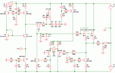
.Test schematic.
I added the 220R base resistors, without them the circuit is prone to oscillations.
As I said without the 1k there is a peak in the response.
Update schematic.
What about this bias scheme ? (similar for Mosfet)
An externally hosted image should be here but it was not working when we last tested it.
I added the 220R base resistors, without them the circuit is prone to oscillations.
As I said without the 1k there is a peak in the response.
Update schematic.
An externally hosted image should be here but it was not working when we last tested it.
What about this bias scheme ? (similar for Mosfet)
An externally hosted image should be here but it was not working when we last tested it.
Perhaps change the direction of the LEDs...Justcallmedad said:
What about this bias scheme ? (similar for Mosfet)
An externally hosted image should be here but it was not working when we last tested it.
Otherwise it looks pretty similar to the one I use.
Ouuups....
Of course led's are inverted !, As they where just illustration schematics, I didn't care in drawing them, sorry.
Iam enjoying listening the mosfet circuit, it really sings
For the moment I use it with a PCM63 DAC and it makes a real difference compared to the 100R I/V resistor!
Of course led's are inverted !, As they where just illustration schematics, I didn't care in drawing them, sorry.
Iam enjoying listening the mosfet circuit, it really sings
For the moment I use it with a PCM63 DAC and it makes a real difference compared to the 100R I/V resistor!
Nice work !!!
I am bit confused now, could you please make clear WHICH mosfet circuit you just referred to?
Extreme_Boky
Iam enjoying listening the mosfet circuit, it really sings
I am bit confused now, could you please make clear WHICH mosfet circuit you just referred to?
Extreme_Boky
What do you think of the difference to the original I-V stage?Justcallmedad said:
Iam enjoying listening the mosfet circuit, it really sings
For the moment I use it with a PCM63 DAC and it makes a real difference compared to the 100R I/V resistor!
Just wonder since I used the same DAC with my new I-V stage.
What do you use as a buffer at the output?
Extreme_Boky:
I am bit confused now, could you please make clear WHICH mosfet circuit you just referred to?
I referred to the circuit in post 22 “Update schematic”.
As I mod also the reference for the mosfet, the new schematic (for the moment
) is the one below (the one I am listening to).Nicke:
What do you think of the difference to the original I-V stage?
If you mean with the AD844… it’s another world, if you mean vs. an I/V resistor it’s about the same musicality and transparency but much more detailed as well as much more deeper and precise bass.
I don’t use any buffer for the moment I just pick up the output, at the 1k resistor R8.
I am working on it, probably a fet follower with offset correction (somethink like I used on "Output stage for Sony cd players", as soon as I test it, I will post schematics.
Actual circuit:
An externally hosted image should be here but it was not working when we last tested it.
And here the FFT graphs, THD 3.145 kHz and IMD (250 Hz/ 8kHz).
THD 0dB.
THD –10dB.
IMD 250Hz/0dB - 8kHz/-10dB.
IMD 250Hz/-10dB - 8kHz/-20dB.
As always any comments, suggestions, or hints are welcome
Perhaps a resistor at the gate of the MOSFETJustcallmedad said:
As always any comments, suggestions, or hints are welcome
And some more current in the input stage...
Nicke said:
Perhaps a resistor at the gate of the MOSFET
And some more current in the input stage...
The resistor at the mosfet gate isn’t necessary, this is "done" by R8
.Actually both stages run at 8 mA, do you think it’s not enough, 10 times the delta DAC output ? (+/-0.75 mA). I am talking about the AD1853, but for the PCM63 you are probably right, +/- 2 mA. Have you listen compared vs. differents bias currents ?
Sorry, in post 26 you speak about the original circuit,I thought that you where referring to the B.B./Elektor PCM63 output stage circuit… and not about the "Simple I/V stage" from Jocko vs. the one with folded cascode mosfet, in this case I can't say. I just built and listened to the circuit as in post 28, in the simple I/V circuit a capacitor is essential... For me is just an example of I/V conversion not a "full operating circuit", I could try one of these days.
I have in mind for DC-Servo, something like the circuit below. …If I correctly understand Jocko’s lesson…
The Mosfet and the circuit around it, replaces Q5 ccs in my last schematic (post 28). I will complete it after the design of the output stage buffer and with all the balanced input/output circuit.
DC-Servo:
An externally hosted image should be here but it was not working when we last tested it.
Justcallmedad said:
And here the FFT graphs, THD 3.145 kHz and IMD (250 Hz/ 8kHz).
As always any comments, suggestions, or hints are welcome
Hi,
can you post FFT with -60 dB ?
Would be interesting for me...
It is probably right but the reason I suggested it was to lower input impedance.Justcallmedad said:
Actually both stages run at 8 mA, do you think it’s not enough, 10 times the delta DAC output ? (+/-0.75 mA). I am talking about the AD1853, but for the PCM63 you are probably right, +/- 2 mA.
No...not yet......Justcallmedad said:
Have you listen compared vs. differents bias currents ?
The one I meant was the original Elektor version with AD844 as I/V.Just wondered if you had the same experience like I did(a big improvement with a new I/V stage).Justcallmedad said:
Sorry, in post 26 you speak about the original circuit,I thought that you where referring to the B.B./Elektor PCM63 output stage circuit… and not about the "Simple I/V stage" from Jocko vs. the one with folded cascode mosfet, in this case I can't say. I just built and listened to the circuit as in post 28, in the simple I/V circuit a capacitor is essential... For me is just an example of I/V conversion not a "full operating circuit", I could try one of these days.
It will be interesting to the measurements when you make a differential version of the I/V stage...It shouldn´t be very much distortion left...
Bernhard said:
Hi,
can you post FFT with -60 dB ?
Would be interesting for me...
Of course I can carry this measure, but I would prefer to know under which conditions.
What would interest you, the I/V circuit performance at -60 db or the overall DAC + I/V circuit performance?
Could you explain more precisely in what you are interested for…
Nicke said:
It is probably right but the reason I suggested it was to lower input impedance.
No...not yet......
The one I meant was the original Elektor version with AD844 as I/V.Just wondered if you had the same experience like I did(a big improvement with a new I/V stage).
It will be interesting to the measurements when you make a differential version of the I/V stage...It shouldn´t be very much distortion left...
I don’t think that increasing current, even double it could make a such difference in the input impedance for the DAC, I believe that it depends more on the bjt device used.
I can try some measures in this way, but I think that it will not be so easy…
About the improvement over the AD844, or even a simple resistor vs. "Jocko's" circuit, absolutely agree with you!
Right, in the differential version I expected less THD, especially THD2, even if this one is not so important for sound quality, but it could generate harmonics in the others components of the audio chain.
Justcallmedad said:
What would interest you, the I/V circuit performance at -60 db or the overall DAC + I/V circuit performance?
Could you explain more precisely in what you are interested for…
More the overall performance*, I think at low level the DAC chip itself is dominating.
I was not satisfied with PCM63 all grades.
Now I got another PD8500 with J grade PCM63 made in USA, not tested yet.
* That does not mean I`m not interested in your I/V stage, but generally before I have to find "my" chip.
Bernhard said:
More the overall performance*, I think at low level the DAC chip itself is dominating.
I was not satisfied with PCM63 all grades.
Now I got another PD8500 with J grade PCM63 made in USA, not tested yet.
* That does not mean I`m not interested in your I/V stage, but generally before I have to find "my" chip.
For Bernhard some PCM63 measures:
PCM63 -10dB 1 kHz.
PCM63 -50dB 1 kHz.
I am here to share, learn and when I can help people to get best sound, infact best music reproduction, it represents for me a great pleasure and I know that this is the case of most people around here, so no problem if I can do the measures, even if you are not interested by I/V stage, I sell nothing especially in this field, I expect the same from the other people here, except those who are involved in this job and must protect their knowledge to exist so to give pleasure for non DIY people, but I must say that sometimes (when they can) their hints are very useful.
---------------------------------------------------------------------
I took some measurements on the common base circuit input impedance vs. various idle currents:
04 mA Zin = 7.3R
08 mA Zin = 3.8R
16 mA Zin = 2.4R
I think, but I could be wrong, that 8 mA is a good compromise between input impedance, linearity and noise, with 2SC2547 or 2SC2240.
- Status
- This old topic is closed. If you want to reopen this topic, contact a moderator using the "Report Post" button.
- Home
- Source & Line
- Digital Source
- Another I/V stage…