Question for the gurus here:
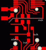
On the board below, I have clocks coming in from the left and being distributed to two ICs. The pads you see are 50R resistors. SDATA, LRCK, and BCK are all relatively low-frequency clocks, but MCK is running at 24.576MHz.
My question is about how best to route MCK. The desired path is indicated by the brown line, and I could push it through almost as depicted, but I am concerned about crosstalk.
Other options would be jumpering MCK over this block via the topside, or under the board.
As for routing on the bottom layer, I am concerned about routing under clock lines. Routing completely around these blocks would create very long traces, which is not an option.
How would you route this signal?
Attachments
PCB design
Hi Tiroth
I would route it as indicated but use through hole resistors. This will give more clearance.
I recognise the situation; you have forced yourself in a tight corner making it difficult to route the last trace. Widen up the design.
As MCK and the othet clock dsignals are perpendicular to each other you will have minimal interaction.
")
Hi Tiroth
I would route it as indicated but use through hole resistors. This will give more clearance.
I recognise the situation; you have forced yourself in a tight corner making it difficult to route the last trace. Widen up the design.
As MCK and the othet clock dsignals are perpendicular to each other you will have minimal interaction.
Hi Tiroth,
You seem to be busy, hu ?
I think the solution relies on the resistors. Sorry Elso, but I don't think using THT resistors would be a good idea. They add a lot of inductance, whithin the resistor itself, and with the leads too.
If I understand clearly from your drawing (hard to see without parts' silouhette), you drive two resistors with one signal (let's call this side the input), and the other side of the resistors (let's call 'em outputs) feeds the two ICs (which ones, I wonder) separately.
If I'm right in my deductions, I think you'd better use a SMT resistor array. Vishay makes nice ones with a 50 mils or 25 mils pitches, which would fit nicely on you board as they look like SOIC or SSOP packages (Sorry, I do not have any link or reference handy, but I'll post it as soon as I refind it). The advantage is that they provide some space beneath them (more than a 0805 or 1206 part) that allow you to route some signals under the part. As a drawback, this implies that you also route MCK through this array...
And speaking of crosstalk... Trying to avoid it is a nice rule (and I also try to do it), but I wonder what happens inside an IC with a 26 mils pitch...
Hope this helps
You seem to be busy, hu ?
I think the solution relies on the resistors. Sorry Elso, but I don't think using THT resistors would be a good idea. They add a lot of inductance, whithin the resistor itself, and with the leads too.
If I understand clearly from your drawing (hard to see without parts' silouhette), you drive two resistors with one signal (let's call this side the input), and the other side of the resistors (let's call 'em outputs) feeds the two ICs (which ones, I wonder
) separately.If I'm right in my deductions, I think you'd better use a SMT resistor array. Vishay makes nice ones with a 50 mils or 25 mils pitches, which would fit nicely on you board as they look like SOIC or SSOP packages (Sorry, I do not have any link or reference handy, but I'll post it as soon as I refind it). The advantage is that they provide some space beneath them (more than a 0805 or 1206 part) that allow you to route some signals under the part. As a drawback, this implies that you also route MCK through this array...
And speaking of crosstalk... Trying to avoid it is a nice rule (and I also try to do it), but I wonder what happens inside an IC with a 26 mils pitch...
Hope this helps
Elso,
I didn't expect you to have problems. What I just meant is that when frequency increases, parts do not behave as ideal ones, and parasitic (R, L, C) can ruin a lot of efforts. And SMT parts usually have lower parasitics than THT ones. I'm sure you can obtain even better results with your asynchronous reclocker if you try to build it with only SMT parts (knowing you, perhaps you've already tried, hu ?).
I didn't expect you to have problems
. What I just meant is that when frequency increases, parts do not behave as ideal ones, and parasitic (R, L, C) can ruin a lot of efforts. And SMT parts usually have lower parasitics than THT ones. I'm sure you can obtain even better results with your asynchronous reclocker if you try to build it with only SMT parts (knowing you, perhaps you've already tried, hu ?).general thoughts on clock crosstalk
Slower clocks still have the same edge speed, so they might produce almost the same amount of crosstalk as a higher frequency clock. As they are synchronous to MCKL and do not contribute to timing accuracy (maybe with the exception of WDCLK on older multibit DACS), I would not worry about crosstalk into them.
On the other hand, SDATA is synchronous to MCKL (albeit with some delay), but also aperiodic, hence it might induce pattern-dependent crosstalk into MCKL, i.e. the device receiving the MCKL might detect the edges at different times depending on what data there is on SDATA.
In a modern system with an integrated filter DAC I would suggest the following scheme: use a high quality oscillator close to the DAC and route the clock through a buffer with a well-decoupled supply, using no or only a small series impedance in this line. A separate buffer should distribute the clock to all other parts of the circuit. The SDATA (and all other derived signals) should be decoupled at their buffer outputs with a relatively high-value SMD resistor, i.e. 100 - 470 R.
Greetings,
Eric
capslock,
Thanks for the response. All of my clock signals are actually generated at a counter, buffered, with a single line driving two chips per block (the upper and lower ICs in the gif above). The board will have 3-4 of these blocks, so there are constraints on how short clock traces can be made.
Does your statement about series resistance still hold? My thought was that since trace lengths could reach 3-4 inches and pass by other circuit blocks it might be advantageous to decouple all clock lines.
Depends on what those chips do, i.e. if they are jitter sensitive. If you have a modern integrated DAC some place and a master clock close by, all I would worry about is not to corrupt the MCKL clock line that goes from the oscillator to the DAC and controls all internal timing. If you are using a digital filter / multibit DAC approach, the digital filter usually controls the timing of the DACs, but you also reclock the WDCK lines with a 74F74 that is driven from the master clock.
If you don't have a master oscillator and all those nice chips are part of a semi-discrete PLL, my statement would probably not hold.
I like to use a small series resistance (20 - 90 R) on critical lines because it keeps the worst switching transients from the receiving input. If it is too large, the edges become even cleaner but are so round the input gate has too much freedom to decide when it is time to switch. The same goes basically also for non-critical inputs on the same chip because the input gate draws a high current while the signal is between valid states.
For non-critical input on other chips all you have to worry about is that the digital information gets transmitted correctly, so you have to look at the setup times given in the timing diagrams. In many cases, you can get away with 1 k.
Eric
clock routing
Capslock,
Having but very limited experience in this area, can I pick your brain?
Why is a buffer between the clock and the DAC or whatever good to minimize jitter? Wouldn't there be a chance that the buffer itself generates jitter? After all, it is just another bunch of gates that have to switch states at some point on the rising/falling edge.
Thanks for any clarification.
Jan Didden
Jan,
you are right that a buffer is bound to add some jitter. But let's consider how an oscillator works:
In many cases, there will be one or a few transistors that provide the gain that makes the crystal oscillate. The output is usually sinusoid which few DACs can accept and which is vulnerable to contamination if transmitted over a line due to its slow risetime. Therefore, one would use a comperator or logic gate to make this a square wave. This is already a buffer and would therefore work. This is in fact a configuration that one sees often enough. However, on its input this device sees a slowly changing signal and it has to decide when to switch. So a couple of µV of noise on the input circuit that couple from the output capacitively or through the internal power supply rails would already result in several dozen ps jitter.
Hence it would be a better idea to load this "rectangularizing" gate as lightly as possible, i.e. with another buffer. It might even be a good idea to use several buffers to drive the DAC and the other non-critical parts of the board. These should not be within the same device lest nasties on the longer lines couple back into the buffer that drives the DAC.
For oscillators without a transistor , i.e. topologies where the gate (TTL, ECL, comparator) also drives the crystal, it is even more advisable not to load the output with anything else.
Although I haven't seen figures I would also expect a TTL gate to be much less jittery when driven from a high-slew-rate signal compared to something slower that is just within spec. The reason is again that the transition time trough the threshold region where noise may have an effect is much shorter for a fast signal. One should, however, limit overshoot that might cause the protection diodes to conduct by using a small series impedance.
Clear enough?
Eric
Clock routing etc
Eric,
Yes, thanks, very helpfull.
As I said, this is not my area of expertise. I more or less assumed that the *squaring circuitry* would be included on the oscillator chip or whatever. Also, using a series resistor one would probably want to take a look at the capacitive load at the driven circuitry to avoid slowing down the rise times again, I guess.
Do you have any info on the shift of the switching point of a gate with time or with temperature? I know it varies from gate to gate, but does it vary over time/temperature for a particular gate?
Cheers, Jan Didden
- Status
- This old topic is closed. If you want to reopen this topic, contact a moderator using the "Report Post" button.
- Home
- Source & Line
- Digital Source
- Clock routing dilemma