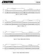
This is what I want to know. I've searched the forum, but I never really found a clear explaination of each. Reason I ask is because I'm not sure about the format that the Toshiba TC9231N accepts. It's an ols obselete S/PDIF transmitter. According to the datasheet, it accepts the EIAJ Digital Audio Interface.
Here is a waveform diagram of what the TC9231N will accept.
It converts this to S/PDIF. Because this IC is obselete, I found the CS8405A to replace it, but I'm not sure what the format of the source I am going to use is. I'm guessing Left justified, but I could be wrong. It doesn't look like an I^2S waveform. Any info would be greately appreciated.
Thanks.
Here is a waveform diagram of what the TC9231N will accept.
An externally hosted image should be here but it was not working when we last tested it.
It converts this to S/PDIF. Because this IC is obselete, I found the CS8405A to replace it, but I'm not sure what the format of the source I am going to use is. I'm guessing Left justified, but I could be wrong. It doesn't look like an I^2S waveform. Any info would be greately appreciated.
Thanks.
Hi Emuman,
As I recall it, I2S updates the data bits on the falling edge of the clock. Looks like your timing diagram does just that.
It also looks like your waveform is both left justified and right justified at the same time. You have exactly one data word for each phase of the LR clock. It's not like you have non-data bits before (right justified) or after (left justified) the actual data.
What is the signal source that produces your data? Will you use an external clock soruce or generate the timing in a programmed device?
I have some experience using FPGAs with SPDIF receivers and external clock sources. What I do there is poll for clock edges and count bits. When an edge of the LR clock (or frame sync) is detected, I latch the data and force a counter reset.
A little tip I got from a friend of mine: You might want to poll for the non-intuitive clock edge before reading bits. In the timing diagram, data is updated on the falling edge, and steady at the rising edge. But by the time your FPGA or processor or whatever has detected the rising edge, a falling edge may already have occured, and your signal is not valid. Thus if something fails, try polling for the falling edge and gamble on the signal being stable by the time your FPGA becomes aware that the falling edge occured.
Hope this helped. It is hard to help you any more without knowing more about your application at the time.
--
Børge
Thanks guys.
It seems to me that the only difference between i2s and left justified is that the word clock is inverted with left justified in respect to i2s.
The source, of course, is the nintendo gamecube. The TC9231N circuit has the word clock inverted, but the data and bit clock are just buffered with CMOS SN74HC04. Will the buffering affect anything? I personally see no use for it other than to protect the source. I bet it adds jitter too. In most designs with CMOS inverters I've seen, they are not used to buffer any signal. I want to use the CS8405A in place of the TC9231N and have redrawn the design according to cirrus's recommendations. I don't see the need to buffer or invert the S/PDIF output either. What would be the need for that?
Thanks.
- Status
- This old topic is closed. If you want to reopen this topic, contact a moderator using the "Report Post" button.