I have been pondering different IV stages for my small tda based nos dac.
As space is an issue I have been using a passive arrangement thus far.
I am tempted just to try something OP based as per data sheet,
but note there seem to be many views on best practice for IV conversion.
I am wondering whether there was any value in using a low value
IV resistor passive conversion [as I understand the dac would prefer to see the lowest impedance possible] and following it with a couple of op amp stages to amplify the output voltage to usable levels?
Setmenu
Hi Carlos
Do you think such an approach would potentially sound better than using the data sheet OP Based Iv conversion?
I have looked over some discreet designs and they would be
hell to fit into the small space I have available.
And it does seem that the 'best' ways are the most bulky

To my noob understanding at least.
Cheers
Setmenu
Do you think such an approach would potentially sound better than using the data sheet OP Based Iv conversion?
I have looked over some discreet designs and they would be
hell to fit into the small space I have available.
And it does seem that the 'best' ways are the most bulky
To my noob understanding at least.
Cheers
Setmenu
setmenu said:Hi Carlos
Do you think such an approach would potentially sound better than using the data sheet OP Based Iv conversion?
Let's say it's a good solution for your problem.
or this?
may need a buffer at the output.
An externally hosted image should be here but it was not working when we last tested it.
may need a buffer at the output.
Thanks for the input folks.
Perhaps I ought to study a bit more before I post questions in these forums ,as one problem here is one of lack of basic knowledge
My experience of ground up discreet design is, well zero...
Most of what I have made is data sheet and from the hard work of others.
Therefore...Till I don't really understand schematics such as your
example too well

So I cannot answer your question
Setmenu
Perhaps I ought to study a bit more before I post questions in these forums ,as one problem here is one of lack of basic knowledge
My experience of ground up discreet design is, well zero...
Most of what I have made is data sheet and from the hard work of others.
Therefore...Till I don't really understand schematics such as your
example too well
So I cannot answer your question
Setmenu
setmenu said:"Thanks for the input folks.
Perhaps I ought to study a bit more before I post questions in these forums ,as one problem here is one of lack of basic knowledge
My experience of ground up discreet design is, well zero...
Most of what I have made is data sheet and from the hard work of others.
Therefore...Till I don't really understand schematics such as your
example too well
So I cannot answer your question
The above aside, I would be grateful if you would not mind placing yourself [briefly] in the role of teacher, as I would be most interested in a description of how the circuit functions.
I do of course realize forums such as this are intended for frank discourse and exchange of ideas rather than to hand hold beginners.
Cheers
Setmenu

i really do not feel like beeing the one to teach electronics - i´m a dilletant in thise area.
Its only, i had the same thoughts about resistor I/V conversion with low resistor value and amplifier to get usefull voltage level out of the DAC.
I did not test the circuit in real world, but ordered some jfets to play with.
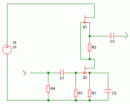
The DACs current output should be represented by the AC source shown "AC sine 1 0 .... " with the 1k resistor behind. Out of this resistor comes something like AC current ~ 1mA p-p, what is our DACs output for simulation.
This current is flowing through R4 to GND (or whatever voltage level the DAC likes) and makes an AC voltage across R4 which is AC coupled with C1 in an voltage amplifier formed by the 2 Jfets. C3 couples out the C portion of voltage that appears at Q1 source were i hope to find some voltage swing and lowest output impedance. R5 represents the next amplifier stages input impedance (preamp or buffer stage) and "probe 1 - Node" shows the amplified voltage swing. Its around +-2 V with the 47k at R6.
Function of the amplifier you will see when thinking about how the Jfet works: it is open with difference between gate and source = 0 and closes with gate going more negative than source, closed at some transistor dependend voltage like 2 Volts or so. (see diyopamp at passdiy) The voltage difference is the voltage across the resistor between gate and source, and this difference is caused by the current through the resistors.
Jfet choosen with hope for low noise. Circuit choosen for beeing simple low parts count and without feedback loop.
I don´t know if it will work, if it will be good or crap. Some more experienced members will comment on this... Also i hope they will correct mistakes i made in circuit and explanations.
Its only, i had the same thoughts about resistor I/V conversion with low resistor value and amplifier to get usefull voltage level out of the DAC.
I did not test the circuit in real world, but ordered some jfets to play with.
The DACs current output should be represented by the AC source shown "AC sine 1 0 .... " with the 1k resistor behind. Out of this resistor comes something like AC current ~ 1mA p-p, what is our DACs output for simulation.
This current is flowing through R4 to GND (or whatever voltage level the DAC likes) and makes an AC voltage across R4 which is AC coupled with C1 in an voltage amplifier formed by the 2 Jfets. C3 couples out the C portion of voltage that appears at Q1 source were i hope to find some voltage swing and lowest output impedance. R5 represents the next amplifier stages input impedance (preamp or buffer stage) and "probe 1 - Node" shows the amplified voltage swing. Its around +-2 V with the 47k at R6.
Function of the amplifier you will see when thinking about how the Jfet works: it is open with difference between gate and source = 0 and closes with gate going more negative than source, closed at some transistor dependend voltage like 2 Volts or so. (see diyopamp at passdiy) The voltage difference is the voltage across the resistor between gate and source, and this difference is caused by the current through the resistors.
Jfet choosen with hope for low noise. Circuit choosen for beeing simple low parts count and without feedback loop.
I don´t know if it will work, if it will be good or crap. Some more experienced members will comment on this... Also i hope they will correct mistakes i made in circuit and explanations.
Hi Till
I very much appreciate you taking the time to explain this to me .
I will now endeavor to broaden my own knowledge of these things, as I find the idea of a minimalist discreet iv stage that is
dac friendly rather appealing.
my initial consideration was to use a dual op package to create
a multi gain stage for the tiny v that would be present at a low
value IV resistor.
This would not necessarily be as compact as something along the lines of your circuit though.
At present I am trying to get my head around M.O.J Hawkford's
paper on : current steering transimpedance amplifiers for High resolution DA converters.
Seems interesting, That is what I understand of it !
Nothing like trying to run before you can walk eh?
Cheers
Setmenu
I very much appreciate you taking the time to explain this to me
.I will now endeavor to broaden my own knowledge of these things, as I find the idea of a minimalist discreet iv stage that is
dac friendly rather appealing.
my initial consideration was to use a dual op package to create
a multi gain stage for the tiny v that would be present at a low
value IV resistor.
This would not necessarily be as compact as something along the lines of your circuit though.
At present I am trying to get my head around M.O.J Hawkford's
paper on : current steering transimpedance amplifiers for High resolution DA converters.
Seems interesting, That is what I understand of it !
Nothing like trying to run before you can walk eh?
Cheers
Setmenu
- Status
- This old topic is closed. If you want to reopen this topic, contact a moderator using the "Report Post" button.
- Home
- Source & Line
- Digital Source
- Low value IV resister followed with high gain amp stage?[tda1543]