Hi all,
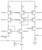
Inspired by Jocko's simple iv stage and Bricolo's suggestion , which he scrapped when the input impedance was too high. I thought a bit on how to fix the input voltage to a fixed value.
I am not sure this circuit works in real life but in simulation it performs quite good. ~-70db THD at 10k
If i replace the transistor models with sa970 and sc2240 instead and optimize the resistor values and look at 1k it says ~-90dB THD, third order dominating.
Now i do not beleive distorsion measurements in simulations but they are the only thing i have.
Can anyone comment on the concept at least, does it work at all. A friend of mine said the startup could be problematic and might require extra circuitry i.e if there is no current there is no way to get a current.
The idea to lower the input impedance lied in the fact that the Vbe is correlated to the Ic so i needed to copy the Ic of the input transistor to the one supplying the reference point to the input transistor base this meant i couldnt take this current to drive a output so i mirrored the current both ways and got fairly good results.
The circuit works down to +-5v if you limit the output swing but +-15 seems to give better distortion figures. The emitter resistors of both the input and the "mirror" are not equal to acheive optimum performance on both distortion and inout impedance.
R4_10 is slightly bigger than R4_9 and R4_11 to compensate for the base currents in the mirror. The R1_12 is a bit bigger than R0_13 to compensate for different currents in the devices.
The cascode on the output isn't necessary but the distortion went down a lot when i included it, optimum seems to be to place it some 4V from the rail (less if the rail is 5V of course).
Looking at transient step responses it looks very controlled and settles nicely.
If anyone wants to i'll post the simulation files, spice cir files.
And to intercept all those who will say just go build the damned thing and measure it, i would if i had the time, too many kids and dogs requireing attention! All i have time to do is come up with ideas and try them out in a simulator, i do not even have the measurement equipment to do the measurements.
Anyway here it is and if this is nothing new then just ignore my mad ramblings.
Attachments
If you want to go with current mirors, Mr Hawksford has a good article about IVs, and on page 20 you'll find a very well designed one based on mirors.
It uses a 1:1 miror, and a buffer after the I/V resistor. But there's certainly a possibility to modify it into a 1:3 or more curent miror
http://www.essex.ac.uk/ese/research...Current steering transimpedance amplifier.pdf
It uses a 1:1 miror, and a buffer after the I/V resistor. But there's certainly a possibility to modify it into a 1:3 or more curent miror
http://www.essex.ac.uk/ese/research...Current steering transimpedance amplifier.pdf
Iv
Hi hjelm,
I agree with Jocko that the inputimpedance should be as low as possible. The common base amplifier (also called grounded base) has the lowest input impedance of all three possible configurations. I believe that using a Sziklai pair as input has even lower input impedance, hope so.
I would connect Vref to the base of the input transitor. In your circuit a lot of current goes into the Vref pin.
The folded cascode is a nice way of level shifting and having a extra common-base amplifier.
I think Jocko's circuit is much more elegant as that of the Hawksford guy.
Sure Hjelm, just drop them in, please.hjelm said:If anyone wants to i'll post the simulation files, spice cir files.
Jocko, you kinda should try harder. It can be done better. Trust me.Jocko Homo said:Simualtions are one thing, but in real life, the limit on mine was -80 dB at full output.
Elso, in the circuit you see above (or in the Hawksford's paper) the current mirrored back to the Q1 (or the first transistor of the "super pair" in the Hawksford's paper) yields practical zero input impedance of the circuit (100R-12 resistor must be removed, of course).Elso Kwak said:I believe that using a Sziklai pair as input has even lower input impedance, hope so.
Pedja
Elso,
I didn't test Hawksford's IV yet, so I can't relly tell if it's good or not.
But I've read the article, and in it, he explains every choice he made. And he does this very well, the explanations are easy to understand, and seem very wise.
With all his explanations, he convinced me that the choices were good. That's a good point IMHO
Common base IV
Hi Pedja,
The input impedance is not zero as it should be as the the DAC current source has limited compliance. (Horowitz page 184).
Input impedance of a common base goes down when the collector-emittor current goes up. For example the CB-CB pair in Low Noise Electronic Design, Motchenbacher and Fitchen, has a Ri of 260 Ohm with 100µA of current. But the CB-CC pair with 1mA of current in the CB transistor has an input iimpedance of 29 Ohm.
Pedja said:
Sure Hjelm, just drop them in, please.
Jocko, you kinda should try harder. It can be done better. Trust me.
Elso, in the circuit you see above (or in the Hawksford's paper) the current mirrored back to the Q1 (or the first transistor of the "super pair" in the Hawksford's paper) yields practical zero input impedance of the circuit (100R-12 resistor must be removed, of course).
Pedja
Hi Pedja,
The input impedance is not zero as it should be as the the DAC current source has limited compliance. (Horowitz page 184).
Input impedance of a common base goes down when the collector-emittor current goes up. For example the CB-CB pair in Low Noise Electronic Design, Motchenbacher and Fitchen, has a Ri of 260 Ohm with 100µA of current. But the CB-CC pair with 1mA of current in the CB transistor has an input iimpedance of 29 Ohm.
The thing is that i get a lower zin with the 100ohm resistor since i have the same emitter resistor in the transistor that gives me the reference voltage for the base of the common base transistor.
And it gives me a lower distortion as well.
Consider the case when the current through both the q1 and q2 are the same i get the same voltage drop over the resistors and provided that the Vbe is the same i have 0 volt on the input!
In simulation i trim it down to 110uv PP for 2.4mA PP in.
I admit that the circuit is not very suitable to a Vref other than ground since i feed back the current through it.
Admittedly when the current mirror cannot keep up i will have worse performance on input impedance than without but i choose to do that to get better distortion figures.
Didnt actually read the hawsford paper until now but the concept on the input is similar and yes the Zout is the 1k resistor so it needs a buffer.
I tried this configuration with wilson current mirrors as well but got worse figures, actually they were close but i found out i had made a mistake and when i did the mirrors as they should the distortion increased .
.
And Jocko yes i wish i had the time to build it .
As for the attached files the newivsa970.cir is the one with best performance on input impedance and distortion. The newiv.cir is the version with the BC850C BC860C models unoptimized.
I think there is a need to edit the include lines to adapt the path to the models (the relevant ones are included). The zenermodel include can be deleted.
Thanks for all the answers.
And it gives me a lower distortion as well.
Consider the case when the current through both the q1 and q2 are the same i get the same voltage drop over the resistors and provided that the Vbe is the same i have 0 volt on the input!
In simulation i trim it down to 110uv PP for 2.4mA PP in.
I admit that the circuit is not very suitable to a Vref other than ground since i feed back the current through it.
Admittedly when the current mirror cannot keep up i will have worse performance on input impedance than without but i choose to do that to get better distortion figures.
Didnt actually read the hawsford paper until now but the concept on the input is similar and yes the Zout is the 1k resistor so it needs a buffer.
I tried this configuration with wilson current mirrors as well but got worse figures, actually they were close but i found out i had made a mistake and when i did the mirrors as they should the distortion increased
. And Jocko yes i wish i had the time to build it
.As for the attached files the newivsa970.cir is the one with best performance on input impedance and distortion. The newiv.cir is the version with the BC850C BC860C models unoptimized.
I think there is a need to edit the include lines to adapt the path to the models (the relevant ones are included). The zenermodel include can be deleted.
Thanks for all the answers.
Attachments
Elso,
If I refer to the schematic in post # 1, assume an increase in DAC output current, then the current through the sting of transitors above will decrease, right? The level at node # 12 will tend to rise.
But, the current through the ref string of transistors also decreases because of the mirror action. If Vref is constant, that will decrease the level at node # 13 the same amount as the rise on # 12 would be. The net rise at # 12 is therefore zero (assuming perfect balance and mirror), and a zero voltage rise from a current increase is a zero input impedance. This is obtained by closed loop feedback, not as an inherent circuit attribute.
But that raises another question: why do we need the 100 ohm resistors, since we are talking currents here. They are at best superfluous, at worst limit the dynamic range.
What do you say?
Jan Didden
Consider them the same as emitter degenerators in a current mirror that is where i got the idea to use them at all. The distortion went down in the simulations but i am not experienced enough to know why or if it is true.
Could it lessen the influence of different Vce on q1 and q2?
Reran the simulations and it seems that the distortion is unchanged if i remove them a very small resistor (0.35ohm) was needed to acheive minimum input impedance ~0.6 ohm.
If i am rambling just say so and i will remain quiet.
Could it lessen the influence of different Vce on q1 and q2?
Reran the simulations and it seems that the distortion is unchanged if i remove them
a very small resistor (0.35ohm) was needed to acheive minimum input impedance ~0.6 ohm.If i am rambling just say so and i will remain quiet.
Hjelm,
The 0.35 ohms may be required to balance all those mirrors and their base currents, I haven't looked in detail at that.
There is a difference with the emitter degeneration you mention. That is local feedback mostly used to linearize the Vbe vs Ie characteristic, at the expense of gain (they lower the gain of the stage). You can probably spend many threads here to discuss whether it is better to have low, linear gain with low feedback later on, or high non-linear gain with high feedback later on.
Anyway, your circuit works well because of overall feedback, but I think less than 0.6 ohms is possible with the number of transistors you use. Look at the Hawksford design for instance.
Still, rolling your own is also quite satisfying. I think 0.6 ohms would in practise be low enough to get a very good sounding I/V stage. The voltage excursions with a few mA of DAC current would not upset the DAC.
Jan Didden
Edit: I think a limitation on the performance is the fact that there is an unbalance in the base currents that are added/subtracted in the main input string vs the reference string. That give an unbalance not only in the two currents from the reference and the input, but also in the mirror gain which should ideally be one. If you can play around with that to make those two strings equal in that respect you may make quite an improvement in Zin.
BTW, what exactly is behind Vref?
Vref is ground in my case as i designed towards the pcm1704.
I wouldnt feel comfortable with using this technique for anything but ground as vref but that is only my concern.
Got the rin down to 0.02 ohm but it is like balancing on a knife edge. I removed the 100ohm resistors on q1 q2, rather set them to a low value to avoid having to remove them from the netlist.
Balanced the current mirrors to acheive minimum voltage swing in and low distortion. The optimum was r49 100.865, really tricky to do in real life as the last figure also made an influence.
The optimum for low distortion on R411 was 95.
I can buy that i need to compensate the basecurrents in the left current mirror but why isn't it the same in the right one?
hjelm said:Where is the actual feedback in this circuit? Is it via q1 and Vbe variations?
Yes, the input current changes the Q2 current, which via the mirror coupling and Q1 is returned as Vb correction to Q2. I think people like Cherry would call it a 'transfer resistance circuit'.
Jan Didden
hjelm said:Vref is ground in my case as i designed towards the pcm1704.
I wouldnt feel comfortable with using this technique for anything but ground as vref but that is only my concern.
Got the rin down to 0.02 ohm but it is like balancing on a knife edge. I removed the 100ohm resistors on q1 q2, rather set them to a low value to avoid having to remove them from the netlist.
Balanced the current mirrors to acheive minimum voltage swing in and low distortion. The optimum was r49 100.865, really tricky to do in real life as the last figure also made an influence.
The optimum for low distortion on R411 was 95.
I can buy that i need to compensate the basecurrents in the left current mirror but why isn't it the same in the right one?
Hjelm,
This is interesting as an intellectual exercise, but in practise you will not get so close to balance because the transistors which are identical in a sim will vary all over the place (relatively speaking). Your best bet will be either to use IC transistor arrays and/or make one of the resistors a trimmer.
In practise, what you would do is input an ac signal current into the input and measure the signal voltage at the input. Adjust the trimmer for lowest signal (ideally zero for zero Zin).
Jan Didden
Edit: The right string current is not part of the feedback loop so has no influence on the balance conditions for zero Zin. The right string only determines the DC offset (and the gain of course).
Hawksford's IV
Elso,
I haven't calculated it, but I think the Zin for the Hawksford's IV is an order of magnitude lower than 26R
Look at the schematic, the "input" stage is a sziklai transistor (aka CFP), in fact a cascoded sziklai.
CFP (and not Baxendal's super pair) has a very precisely set Vbe (Vbe of the "big" transistor. Vbe here is the voltage between the base of the grounded one, and the emitter of the "input" one). It's very close to zero (due to local feedback)
And this is even more true here, since both the transistors are running at the same current (there's a "3 legs current miror", one leg for the input transistor+cascode, one for the grounded transistor, one for the output)
As Jocko point out (among others), the transistors in your simulation are 100% identical but this is not the case in real life. Unindentical parts creates distortion, right Jocko?hjelm said:I am not sure this circuit works in real life but in simulation it performs quite good. ~-70db THD at 10k
If i replace the transistor models with sa970 and sc2240 instead and optimize the resistor values and look at 1k it says ~-90dB THD,
BTW: Have you thought making a current feedback amp in I/V mode? You can check here
if you want to get inspired. It may be hard to succeed without any feedback or bias stabilization.Have you checked BC847BS, cheap dual transistors.
An externally hosted image should be here but it was not working when we last tested it.
An externally hosted image should be here but it was not working when we last tested it.
- Status
- This old topic is closed. If you want to reopen this topic, contact a moderator using the "Report Post" button.
- Home
- Source & Line
- Digital Source
- Yadis: Yet another discrete IV stage