I've been thinking about this for a long time coming and its finally dawned on me that I might be able to actually start this.
The plan sofare is to create a handheld DSO capable of doing pretty much anything and more of its analog equivalent (cheating of coarse).
I'm not too interested in all the extras i can incorperate through software at the moment since it would be useless without some base hardware to develop for.
Sofare the specs stand at -
DS89C450 - 4 8 bit IO's, 64kb of program memory, 33 MIPS @ 33 Mhz
SN74V3690 - synchronus FIFO, 32768 x 36bits, 133Mhz max, 5v tolerant
2x ADS5500 (or slower equivalent) - 14 bit ADC, 125MSPS
Graphic lcd of some undecided size
The uC I chose should, by all means, be fast enough to display everything. The FIFO acts as a storage buffer with the ADC's constantly running whether the FIFO is full or not. Once a refresh needs to take place, the FIFO can be reset for fresh data and read by the uC. To have enough room for all the IO's, the FIFO can be read on an 8 bit bus whilst still being able to take data at 36 bits.
The true potensial of such a accurate scope wouldn't be used whilst its outputting to the graphics lcd. If you think about it, even if its 320x240 pixels wide, thats only 320 samples it can fit across the screen at most. The true potensial would be used via USB (or maybe something else??) to connect to a computer to provide, very simply, anything we can possibly do with the ADC data.
The only software issue I'm going to mention is trigering. Do most scopes just trigger at a regular interval or do they try to match the waveform previously sampled?
Optional features such as a logic analyser might be able to be included but IO space is at a premium. If an IO expander is used speed is greatly reduced in most cases which would limit the use of the feature to lower speed logic.
Thing such as input buffers, I don't have alot of information about.
the bitScope site has schematics of thier input buffer, but its only capable of +- 5v. Does anyone know of a better way to get a larger input voltage and/or a way to control the range digitally?
A range of +- 60v would give you 600v with a 10x probe which would be ideal.
heh thats alot of typing...
If anyone has any comment or surgestion please jump in.
I don't mind if you poke holes through my dream whatsoever
Thanks all
Matt
I'm building a scope at the moment, not handheld though but PC based.
The problem with the FIFO method is that you can't have any pretrig (that is save data before the trig point). Instead I use a regular synchronous SRAM as a circular buffer. I save data all the time while waiting for a trig and then I stop a preset number of samples after the trig point. This memory is hooked up to a FPGA that also handles trigger logic, downsampling and other things.
I think the most difficult part of a proper scope design is the analog input stage. Most likely you want:
High input impedance so you can use ordinary probes.
AC/DC coupling
Variable attenuation and amplification so you can change "volts/div".
Variable DC offset.
High bandwidth.
Low noise.
Low temperature drift.
I'm been working on mine for quite a while, and I think I'm getting close. I haven't updated my website with the latest developments in a while, but I will soon (next week probably). It may be of some use to you:
http://area26.no-ip.org/?section=hard&project=scope
cyr said:I think the most difficult part of a proper scope design is the analog input stage. Most likely you want:
High input impedance so you can use ordinary probes.
AC/DC coupling
Variable attenuation and amplification so you can change "volts/div".
Variable DC offset.
High bandwidth.
Low noise.
Low temperature drift.
In addition to all the above, you want "input protection" -- no use spending dozens of manhours designing and building and then fry the thing with the inadvertent application of an over-voltage.
In addition to high input impedance, 50 ohms is nice!
The problem with the FIFO method is that you can't have any pretrig (that is save data before the trig point). Instead I use a regular synchronous SRAM as a circular buffer. I save data all the time while waiting for a trig and then I stop a preset number of samples after the trig point. This memory is hooked up to a FPGA that also handles trigger logic, downsampling and other things.
Is there any benefit in recording events prior the to trigger point?
Is it correct to say most scopes only display the information collected after a trigger point? (I'm definately not 100% on scope operation
 )
)The site you linked off your own site (which i assume your design is based upon) has a very nice input buffer which it seems has taken everything into account. http://www.johann-glaser.at/projects/DSO/analog/
In that design, is the purpose of the DAC to set the 0v reference? (1v in a 2v peak to peak ADC)
In that case can just a standard reference be used?
Maxim now do temperature adjusted reference chips which may simplify things.
thanks for you input sofar
Its very much appreciated
Yes, yes there is definitly a point in being able to record events prior tp the trigger point.
In fact having a flexible triggering system is one of the most important things on any digital data aquisition system/scope, it makes is much more usefull.
Try looking in the manual of a digital scope or data aquistion card(DAQ).
I use a DAQ from National Instruments,NI- 6052E, which has a very nice and flexible system for triggers, you can find the on the NI webiste.
I did some quick research and I now see your point about the FIFO and pre triggers.
For this application, trigger settings have to be done in the digital domain. The only thing is the DS89C450 doesn't have the required speed to search for triggers whilst still retaining a buffer of already examined figures before the trigger point. I can however see a few ways of maybe getting around this.
For measuring repetitive waveforms there has to be an initial trigger event. From this we can calulate frequency, ampliftude, rise/fall times etc. from the collected data as a basis for the next trigger event. In this case, is it safe to assume we can predict the next trigger point and approximate a point before it to start capturing? Then a more exact trigger point can be found by going through the recorded data before the approximate. We can then vary the times prior to the approximated trigger according to the user's input, or by a ratio according to frequency.
For transients, I can only think of the standard logic/threshhold type triggers in order to capture the event accurately but, as you've said, the FIFO won't retain data after it has been written to the uC for display which won't allow pretrigger data to be captured.
i'll get some sleep and thing more about this
Thanks again
Matt
fr0st said:
The site you linked off your own site (which i assume your design is based upon) has a very nice input buffer which it seems has taken everything into account. http://www.johann-glaser.at/projects/DSO/analog/
In that design, is the purpose of the DAC to set the 0v reference? (1v in a 2v peak to peak ADC)
In that case can just a standard reference be used?
Maxim now do temperature adjusted reference chips which may simplify things.
thanks for you input sofar
Its very much appreciated
My design is partially inspired by that one, although I had remarkably similar ideas even before I found that site (great minds think alike
).The biggest flaw with that analog design IMHO, is that it's too complicated. Too many opamps... Also I think having no 1:1 setting on the input attenuator is a waste.
My current design has a JFET opamp (OPA655) on the input, two gain stages (5x and 2x) and drives the ADC single ended. Only three opamps in the signal path.
The DAC is used to set the DC offset, there are two reasons for having it adjustable.
1) Compensate for the offset in the gain stages.
2) DC-shift the input signal to make better use of the ADC resolution when the input isn't centered around 0v.
My design also controls the ADC reference voltage with a DAC, to compensate for gain errors and also provide a little extra "virtual" gain.
My design is partially inspired by that one, although I had remarkably similar ideas even before I found that site (great minds think alike ).
The biggest flaw with that analog design IMHO, is that it's too complicated. Too many opamps... Also I think having no 1:1 setting on the input attenuator is a waste.
With your input relays, do they selected between 1:1, 10:1 and 100:1?
Most of the TI ADC have 2v p2p differential inputs. In the datasheet they show the use of a THS4502 for the differential driving of the ADC from a single ended signal at a gain of 1. If I use that along with a FET input opamp also at a gain of 1, I would have an input stage capable of a max +- 100v? With a 10x probe that allows for +-1Kv to be measured with a resolution of ~0.1v still (using all 14 bits).
From there I could do software scaling in order to fit the waveform to the screen.
I assume thats what you've done for your original DSO.
Do you have the schematic of your final analog stage?
Thanks
Matt
cyr said:
My design is partially inspired by that one, although I had remarkably similar ideas even before I found that site (great minds think alike
The biggest flaw with that analog design IMHO, is that it's too complicated. Too many opamps... Also I think having no 1:1 setting on the input attenuator is a waste.
My current design has a JFET opamp (OPA655) on the input, two gain stages (5x and 2x) and drives the ADC single ended. Only three opamps in the signal path.
The DAC is used to set the DC offset, there are two reasons for having it adjustable.
1) Compensate for the offset in the gain stages.
2) DC-shift the input signal to make better use of the ADC resolution when the input isn't centered around 0v.
My design also controls the ADC reference voltage with a DAC, to compensate for gain errors and also provide a little extra "virtual" gain.
If you look at the Linear Tech application notes for the LTC1446 DAC there is a schematic for autoscaling which you might want to implement.
with respect to offset, there are precision op-amps with auto-offset features (from TI)
if the device is going to have any meaningful bandwidth you might want to consider using op-amps with "disable" function rather than inserting switches in the signal path. TI will send you samples.
When you begin talking of inputs in the 1kV range you are entering into a different strata of measurement and control. Note that some resistors become non-linear over a few hundred volts, note also that with just a little current you can fry a resistor that isn't rated for HV.
fr0st said:
With your input relays, do they selected between 1:1, 10:1 and 100:1?
Most of the TI ADC have 2v p2p differential inputs. In the datasheet they show the use of a THS4502 for the differential driving of the ADC from a single ended signal at a gain of 1. If I use that along with a FET input opamp also at a gain of 1, I would have an input stage capable of a max +- 100v? With a 10x probe that allows for +-1Kv to be measured with a resolution of ~0.1v still (using all 14 bits).
From there I could do software scaling in order to fit the waveform to the screen.
I assume thats what you've done for your original DSO.
Do you have the schematic of your final analog stage?
Thanks
Matt
That's right, 1:1, 1:10 or 1:100 and then 5x or 1x gain, fixed 2x gain and an additional 2x selectable gain by lowering the ADC reference voltage.
I only have the very messy eagle schematic I made when laying out the board for this second prototype. I will draw a clearer, simplified schematic and put it up on my site soon.
Also, it's not actually my final design. I already have some changes planned for the next (hopefully final) version and I will probably make more after some more testing of this version.
Meanwhile, here's a photo of the actual hardware:
An externally hosted image should be here but it was not working when we last tested it.
Note that this 8x10cm board is only the sampling module. There will be up to four of these connected to a "motherboard" with the FPGA and memory.
A closeup:
An externally hosted image should be here but it was not working when we last tested it.
I had a look through most of TI's range of op amps and only a few have a disable function. I'm unsure of how it would be implemented though.If you look at the Linear Tech application notes for the LTC1446 DAC there is a schematic for autoscaling which you might want to implement.
with respect to offset, there are precision op-amps with auto-offset features (from TI)
if the device is going to have any meaningful bandwidth you might want to consider using op-amps with "disable" function rather than inserting switches in the signal path. TI will send you samples.
When you begin talking of inputs in the 1kV range you are entering into a different strata of measurement and control. Note that some resistors become non-linear over a few hundred volts, note also that with just a little current you can fry a resistor that isn't rated for HV.
If you disable the opamp the output goes into a high impedence state, so the only way switching gains would be to cascade to opamps and have one on whilst the other is off. Swithcing between them will cause the switch in gain, the only thing is, if you cascade them the external components would interfere (well I assume so) because parts of the feedback would be tried to ground which i assume would alter something (frequency respone, output swing, feedback?).
The THS7002 would be an easy way out by sacrificing bandwidth (-3db at 70Mhz). Although its unlikely I'd be measuring a signal greater than 70Mhz it'd still be nice to have the extra bandwidth, but it is an option.
With the auto Offset opamps, do you know which one you are refering to? I had a look at the precision section quickly but none I looked at say the adjusted to drift, but only had very little of it.
Also in relation to measuring a 1kV signal, The input stage should never see the full 1kV. Using a 10x probe, the kV signal is reduced down to 100v and fed to the input stage.
Arn't the ratios 10:1, 100:1 instead of 1:10, 1:100? Otherwise you owuld be amplifying the signalThat's right, 1:1, 1:10 or 1:100 and then 5x or 1x gain, fixed 2x gain and an additional 2x selectable gain by lowering the ADC reference voltage.
I only have the very messy eagle schematic I made when laying out the board for this second prototype. I will draw a clearer, simplified schematic and put it up on my site soon.
Also, it's not actually my final design. I already have some changes planned for the next (hopefully final) version and I will probably make more after some more testing of this version.

Thanks
Matt
fr0st said:
I had a look through most of TI's range of op amps and only a few have a disable function. I'm unsure of how it would be implemented though.
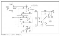
how about this:
Attachments
Another dso project
Hi there,
I am currently doing a prototype dso using THS7530 variable gain amplifier from TI for input stage.
the first DAC7571 sets the gain and the second makes the trig level.
The adc is a ADS831 (8bit - 80 Msps)
The sample clock is generated by an econoscillator from maxim (DS1085).
See the attached schematic.
I am currently evaluating the analog part.
What do you think of this design ?
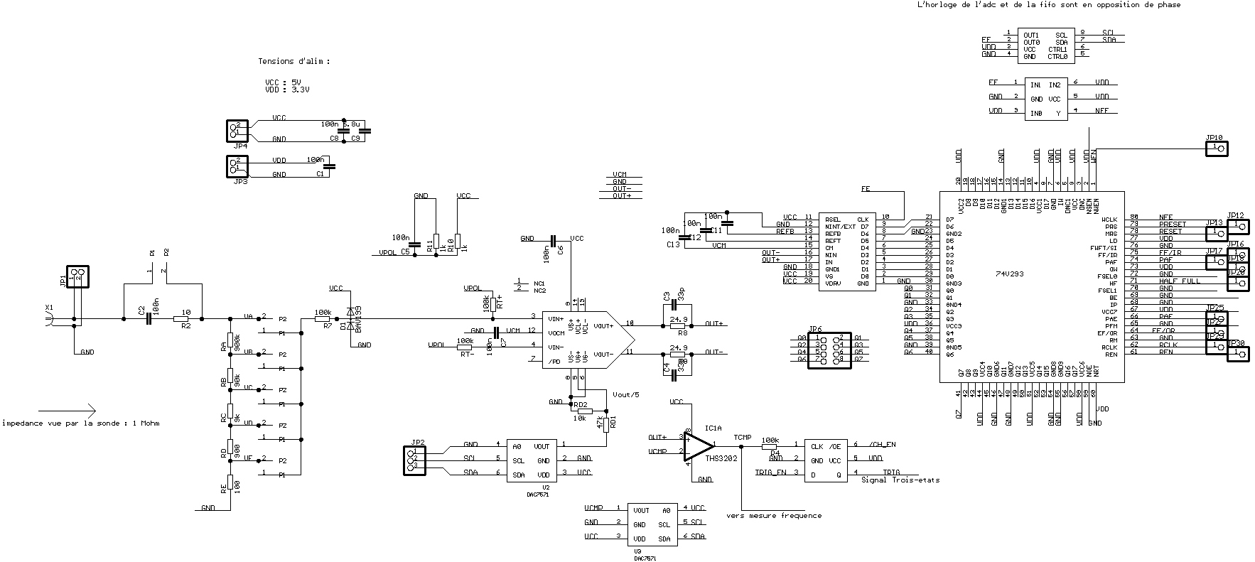
Sorry for the large pic.
Bye
Hi there,
I am currently doing a prototype dso using THS7530 variable gain amplifier from TI for input stage.
the first DAC7571 sets the gain and the second makes the trig level.
The adc is a ADS831 (8bit - 80 Msps)
The sample clock is generated by an econoscillator from maxim (DS1085).
See the attached schematic.
I am currently evaluating the analog part.
What do you think of this design ?
Sorry for the large pic.
Bye
- Status
- This old topic is closed. If you want to reopen this topic, contact a moderator using the "Report Post" button.
- Home
- Source & Line
- Digital Source
- DIYing the Digital Oscilloscope