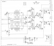
I found some very unusual I/V design in my Philips CD-304MKII:
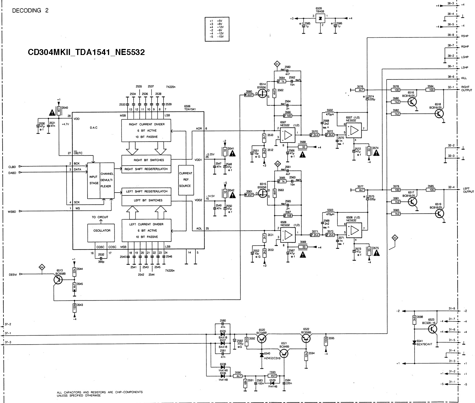
A voltage is fed to the curent output paths (Pins 6 and 25) of the TDA1541 DAC.
Never seen this in an I/V design.
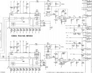
Two curcits shown below, of a Philips CD-304MKII and a CD-960.
Could anyone tell me why?
All the best, Salar
A voltage is fed to the curent output paths (Pins 6 and 25) of the TDA1541 DAC.
Never seen this in an I/V design.
Two curcits shown below, of a Philips CD-304MKII and a CD-960.
Could anyone tell me why?
All the best, Salar
Attachments
I don't think its either of these reasons tbh.
Its not needed for setting any of the DC conditions. The only things I can think of are:
a/ it helps with linearity in some way by forcing a current into that node.
b/ it was found beneficial for some odd start up/shut down issue.
Its not needed for setting any of the DC conditions. The only things I can think of are:
a/ it helps with linearity in some way by forcing a current into that node.
b/ it was found beneficial for some odd start up/shut down issue.
I was going to discount the FET theory but actually its an interesting thought ") It could only be related to the gate drive voltage because the source and drain are tied DC wise.
It could only be related to the gate drive voltage because the source and drain are tied DC wise.
We could do with knowing the DC voltage at the output of the 5532's and at the output of the DAC. Also the FET drive voltage when playing both a disc with emphasis and a standard disc. That should give some clues.
It could only be related to the gate drive voltage because the source and drain are tied DC wise.We could do with knowing the DC voltage at the output of the 5532's and at the output of the DAC. Also the FET drive voltage when playing both a disc with emphasis and a standard disc. That should give some clues.
You make a good case what you say sounds very plausible to get the output in the right ball park. I see there are polar caps used in the signal path and so I'm guessing that the opamp is biased to give a nominally positive bias.
I have an old CD150 upstairs. If it stokes up and runs then I'll measure it and see.
what you say sounds very plausible to get the output in the right ball park. I see there are polar caps used in the signal path and so I'm guessing that the opamp is biased to give a nominally positive bias.I have an old CD150 upstairs. If it stokes up and runs then I'll measure it and see.
It seems both danico and abrax are on the right lines.
I've just measured my old CD150 and it seems the resistors are chosen to add an almost +1v (measured +850mv) offset to the opamp chain. That offset carries through to the final electrolytic coupling cap.
It can't be an 'exact thing' because it uses ordinary resistors fed from a 'nominal voltage' supply. It just gets things in the right zone bias wise.
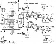
CD-150 hast TDA1540, not 1541.
I looked for other designs - found one with the same deemphasis circuit,
but TDA1541 with LM833 opamp-in this design, the injection is missing.
In a CD304(not MKII) with TDA1540 and NE5532, the injection is missing.
In CD-304MKII with TDA1541 and NE5532, injection ist there.
The datasheets for comparison:
Attachments
Without this resistor there would be 3VDC offset at the opamps before the final coupling capacitor, like in other CD players with this kind of DAC. I still don't get what issue this offset could cause. The output of the DAC is held at virtual ground in either case. We should ask the constructor of this player...
CD-150 hast TDA1540, not 1541............
In a CD304(not MKII) with TDA1540 and NE5532, the injection is missing.
In CD-304MKII with TDA1541 and NE5532, injection ist there.
The CD150 circuit shows the injection present.
I tried to implement a DF1704/PCM1704 circuit instead of SAA7220and TDA541 in a CD-304MKII - just a quick way, cutting the supply line and current output and hooking the 1704 combo on. "Cutting" is not meant literally, luckily the bridges and power supply bead can be unsoldered and used as Connections for the replacements.
But I got no signal at all on the outputs, just a very, very low, distorted signal when shortening current output of the dac to ground by accident.
I do not remember anymore whether I was aware of the injection of 2mA to the TDA1541 DAC at that time. But theoretically, with 2mA offset fed on the current output of a regular DAC like PCM1704, that has NO offset, silence would be not the result, would it?
This current injection will go into the opamp feedback resistor, and will cause its output sit on the negative supply. You need to remove the current injection for a symmetrical output DAC.
Adding a symmetrical DAC and NOT removing the injection - would the logical result be hearing no signal at all?
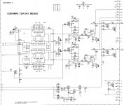
I want to parallel two TDA1541 DACs in a Philips CD304MKII.
Do I have to change the value of the current fed into the L/R outputs?
Or will the usual halving of the I/V resistor´s value do the job?
All the best,
Sal
Addendum: My question at the beginning of this thread was wrong, the current is fed into the opamps´outputs, correct?
Do I have to change the value of the current fed into the L/R outputs?
Or will the usual halving of the I/V resistor´s value do the job?
All the best,
Sal
Addendum: My question at the beginning of this thread was wrong, the current is fed into the opamps´outputs, correct?
OTOH, Nakamichi did feed DC "voltage" to +input of IV opamp.This shift threshold level of TDA1541A's output switches and enable to adjust glitch.read this US5043730 - Digital-analog conversion circuit with application of voltage biasing for ...
Dear Shinja,
thank you very much for your kind help!
The Nakamichi OMS-5 is still one of my favourite players, so it is nice to
find the patent which Nakamichi marketed as "digital deglitching circuit"... correct?
BTW, I still need some Information from Nakamichi. For example who made their front panels. No joke. Brushing and Anodizing an Alumimium
front panel and preserving a glossy, deep black look and smooth surface is a lost art. Even though anodizong is completely different from painting,
the look and feel demanded from Nakamichi was connected to this tradition of Urushi. Europeans never had this heritage of simplified aesthetics.
Todays Front panels are commonly dull and gray. A black panel even fades
In 30years, the anodized black of my nakamichi gear has not faded at all. So if you know one who could give some info...
Back to topic:
My description at the beginning of this thread was right, not wrong as I stated in my last post. 8V are individually fed into the left and right current outputs
of the TDA1541 (Pins 6 / 25) , using two series resistors, one 2k2, one 2k7. The connection between the two resistors is connected to ground using a 10µF electrolytic.
I am not good in math, so I do not know what the resulting voltage/current is. Maybe 2mA or 850mV as stated before.
Now I have an extra TDA1541 and want to parallel it with the existing, both TDA´s will be soldered on a small pcb and decoupled individually.
So current is doubled,I assume that it will be sufficient to halve the value of the Feedback resistor over opamps 6507 and 6508 (1k8 over NE5532).
But will the resistors 3551 and 3553 values need to be halved as well,
to compensate for higher offset?
- Status
- This old topic is closed. If you want to reopen this topic, contact a moderator using the "Report Post" button.
- Home
- Source & Line
- Digital Source
- TDA1541-why is a Voltage fed into the Current Output?