I've done my homework.
Here's a single sided pcb, analog and digital grounds connected. Power supply traces are 40mil, signal is 16 mil. Clearance is 8mil. Grid is 1 inch. I hadn't a correct layout for the inductor, so I used a cap layout. The computer ground is not directly connected to the groundplane but to the chip only.
Here's a single sided pcb, analog and digital grounds connected. Power supply traces are 40mil, signal is 16 mil. Clearance is 8mil. Grid is 1 inch. I hadn't a correct layout for the inductor, so I used a cap layout. The computer ground is not directly connected to the groundplane but to the chip only.
An externally hosted image should be here but it was not working when we last tested it.
An externally hosted image should be here but it was not working when we last tested it.
Gyula--I would have to say that with this single sided board the capacitive coupling from a trace to the ground plane is next to nil. Capacitance between two plates (trace and ground plane for example) is proportional to the area of the plates in parallel, and traces side by side with a ground plane on the same layer are coupled only by the thickness of the 1 ounce copper, NOT the width of the traces.
We do this all the time on low noise photoamps here at work. it works fine, no ground loops. And it's not really a problem with 2 or 4 sided boards either. Calculate the capacitance with 0.062 FR-4 separating two plates, for example (2 sided standard board). It's pretty small. I have in production 4 layer boards (0.015 inch insulating layers between 1 ounce copper traces, 2 signal layers with a ground plane and power plane) with 10 megohm feedback resistors in current-to-voltage converters where 1 picofarad is a big deal. These boards work fine, and the typical parasitic capacitance is on the order of 1/4 picofarad. Not enough to create much of a ground loop....
cheers
Adam
That looks pretty nice, Rookie!
One other comment I forgot to add to the previous post: Ground loops are created when various parts of a circuit have different return paths to ground with significant resistances to those paths. In an extreme case, where a circuit drawing significant current causes a measurable voltage drop across a return trace and shares that ground return with, say, a low level analog signal, real havoc can result--oscillation, noise, etc. As far as the analog circuit is concerned, its ground reference is bouncing up and down as the load varies.
The main reason a fill, or ground plane, is used is so that all the ground return paths are through a large area and thus low impedance conductor, thus insuring that all return paths have a low impedance to ground. And still, if you have a significant current draw (hundreds of milliamps or more), you should have a separate ground plane for the high current circuit only, tied (as I described in the previous post) to the other ground planes where power comes in to the board.
There is a more elegant way to do this--a star ground, where **every** ground path has its own trace back to a single grounding point. I have a picture of a preamp designed by Dan Schmalle (Doc Bottlehead) where every signal or power path has a separate wire, and all the return wires lead to one single point on the chassis. It's definitely a 3-D rats nest and nearly impossible to do properly on a PC board...but technically speaking that is the BEST way to design a circuit. But then again that is why PC boards have ground planes instead...much easier to implement and nearly as effective.
cheers
Adam
Hi Adam!
The ground loop is coming from the parasitic impedance and capacitive coupling. These are the two terms of oscillation. This is not coming from the resistive voltage drop as you wrote, the current division is an another phenomeon. Every path has her own LC, and begin to oscillate with each other.
Gyula
 I just noticed that I forgot to post the schematic
  So stupid..
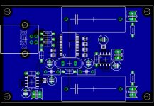
Here we are, what do you think about it ?
Schematic :
Silkscreen :
Top/pads (+ parts outline) :
Bottom (+ parts outline) :
A few comments on the parts.
Chips on board : max1722, dc-dc booster from Maxim, REG102 (5V and 3.3V), low dropout regulator from TI, PCM2702, USB DAC from TI.
Capacitors : C1, C2 are 10uF tantalum. C3, C9 are Pana FC, 1000uF/6.3V. C6, C12 are Pana FC 100uF/6.3V. C15, C16 are ceramic, 32pF. All the other caps are wima mks-02 100nF. 220nF would fit.
Grid is 1cm. The board is about 3cm/6cm (1.2"/2.4").
Schematic :
An externally hosted image should be here but it was not working when we last tested it.
Silkscreen :
An externally hosted image should be here but it was not working when we last tested it.
Top/pads (+ parts outline) :
An externally hosted image should be here but it was not working when we last tested it.
Bottom (+ parts outline) :
An externally hosted image should be here but it was not working when we last tested it.
A few comments on the parts.
Chips on board : max1722, dc-dc booster from Maxim, REG102 (5V and 3.3V), low dropout regulator from TI, PCM2702, USB DAC from TI.
Capacitors : C1, C2 are 10uF tantalum. C3, C9 are Pana FC, 1000uF/6.3V. C6, C12 are Pana FC 100uF/6.3V. C15, C16 are ceramic, 32pF. All the other caps are wima mks-02 100nF. 220nF would fit.
Grid is 1cm. The board is about 3cm/6cm (1.2"/2.4").
2702 layout
Hi again
Took a look at your setup and compared it to the TI eval kit. Interesting, they don't even regulate the voltage input and get their 3.3V with 2 diode drops! pretty crude.....
One thing I noticed on your schematic--you have no pull downs on the audio out. The risk here is that you will get a POP when you plug in the DAC to your preamp and it discharges the output caps. It does not take much load to fix this--I used 330K to ground on each output on my prototype.
I like your power supply scheme. I have several products where I have done just what you propose--a small switcher followed by a linear for good noise performance. Should work fine. Thorsten Loesch has suggested that the TI TL431 is one of the better sounding regulators, might be an alternative to try although I do not know how much difference it will make overall.
On the layout, I would strongly suggest using surface mount components everywhere you can. Especially for all decoupling caps--0805 ceramic caps perform very well and can be put right next to the IC for the best possible decoupling of high frequency noise. Makes the board smaller too!
Nice work!
cheers
Adam
Re: 2702 layout
Thanks for the comments")
Indeed, their version is quite stripped down.aj912 said:Took a look at your setup and compared it to the TI eval kit. Interesting, they don't even regulate the voltage input and get their 3.3V with 2 diode drops! pretty crude.....
True. Well, I could mount the resistors right on the RCA jacks.One thing I noticed on your schematic--you have no pull downs on the audio out. The risk here is that you will get a POP when you plug in the DAC to your preamp and it discharges the output caps. It does not take much load to fix this--I used 330K to ground on each output on my prototype.
Thanks for the comments
Hi, I'm going to build one of these pcm2902-based dacs after reading other people's experiences with it.
I was wondering, does anyone know of software/drivers available that can be used (along with, say, 3 dacs plugged into separate usb ports) for surround sound - e.g route bass/centre, rears and fronts to each dac.
If this could be done it would be nice for movies, games etc (when not listening to stereo audio) .....
Thanks, Pete.
I was wondering, does anyone know of software/drivers available that can be used (along with, say, 3 dacs plugged into separate usb ports) for surround sound - e.g route bass/centre, rears and fronts to each dac.
If this could be done it would be nice for movies, games etc (when not listening to stereo audio)
.....Thanks, Pete.
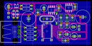
I've sort of taken over development of this board from 00940. Here's a 3D render of the the board I'm going to send off as a beta sometime next week:
I've included pull down resistors (the 0805s near the output), replaced the resistor for the oscillator with an 0805. Also, there's a pad to bypass the switcher or the 5V regulator. All the red caps are WIMA MKS-02 100nF for size reference. The output caps can be Black Gates
If all is well with this board, I'll put a smallish order in for other people
g
An externally hosted image should be here but it was not working when we last tested it.
I've included pull down resistors (the 0805s near the output), replaced the resistor for the oscillator with an 0805. Also, there's a pad to bypass the switcher or the 5V regulator. All the red caps are WIMA MKS-02 100nF for size reference. The output caps can be Black Gates
If all is well with this board, I'll put a smallish order in for other people
g
- Status
- This old topic is closed. If you want to reopen this topic, contact a moderator using the "Report Post" button.
- Home
- Source & Line
- Digital Source
- Pcm2702 Usb-dac