I'm in the process of making an AD1862 dac board and would like some input on how to separate analog and digital grounds.
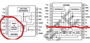
I want to make a single ground plane as Guido Tent recommends, and use proper positioning of the the components to avoid the digital cicuitry creating noise on the analog ground. This is very easy with the AD1865 and the PCM63 chips, as the digital and analog parts inside the chips are neatly separated along the middle. But with the AD1862 it's not so easy. Looking at the datasheet it seems like the lower left part of the chip is used for digital, and the rest is analog. So how do I position two chips next to each other without mixing the grounds?
The only way I've managed to solve this problem is to make separate mono dac boards. I've created the circuit on a prototype board. It works fine with a mono board. Very low noise. But with two dacs side by side on one board, the left channel gets really noisy.
Any input on this subject is very welcome.
Attachments
No decoupling caps next to the power pins, especially on the digital side, some small package 100nF.
C1 C2 should be as data sheet C1 X10 C2s value.
You run the analogue out (P11) through the digital section!
Could you post your schematic and any mechanical constraints, as I think a complete rethink of the layout may be in order.
The analogue out, I would run as pseudo balanced to the next device in line (an op-amp?).
on site at the moment but will be at home at the weekend, have a bit of a layout to finish for someone else, then I will dig you out some practical examples of what I mean.
Marc
No decoupling caps next to the power pins, especially on the digital side, some small package 100nF.
C1 C2 should be as data sheet C1 X10 C2s value.
You run the analogue out (P11) through the digital section!
Could you post your schematic and any mechanical constraints, as I think a complete rethink of the layout may be in order.
The analogue out, I would run as pseudo balanced to the next device in line (an op-amp?).
on site at the moment but will be at home at the weekend, have a bit of a layout to finish for someone else, then I will dig you out some practical examples of what I mean.
Marc
Thanks for the quick reply!
The cap value choices are based both on sidiy's cd player project on diyhifi.org, and on Guido Tent's white paper on decoupling.
The 4,7uF and 47uF C1 and C2 are both in line with the recommendations in the datasheet; "The ratio between C1 and C2 should be approximately 10. Additional noise reduction can be gained by choosing slightly higher values for C1 and C2 (...)"
I have omitted the 100nF decoupling caps to avoid the ringing of parallel caps, shown in measurements here on the forum. This is also Guidos recommendation. But of course, I can experiment with some 100nF ceramics.
And then about the layout. I placed out all the caps first, in order to create the minimum return path from the supply pin to the respective ground pin. After that there was no other way to route the Iout trace. Is it that bad running the Iout trace between the VL+ and the TRIM pin?

The IV stage will be a discrete BJT, similar to Jocko and rbroer. Preferably on the same PCB. How would you implement a pseudo-balanced inteface? I have to admit I'm not even sure what you mean by pseudo-balanced in this case.
I'll post the schematic when I have access to it. As for mechanical constraints, there are none.
Any practical examples would be highly appreciated. I'm curious how you would rethink the entire layout.
Below is the hyperlink to an ADI app. note addressing this subject.
http://www.analog.com/static/imported-files/tutorials/MT-031.pdf
http://www.analog.com/static/imported-files/tutorials/MT-031.pdf
Sorry read the 4.7 as 47.
You need 0.1uF (MLCC, X7R preferably SMD) caps next to the power supply pins, as per the data sheet and common practice with all digital designs, in the smallest possible case. Without them you only have reservoir caps.
I can provide you with a whole host of information on decoupling....There is a lot more info out there since that was written, and clock speeds, rise times and just general density of PCBs has increased greatly in the last few years, as has EMC problems increased, it is an area I have studied quite intently over the last 28 years, as well as EMC.
As said earlier I am stuck on a customers site so cant do any practical examples till tomorrow/Saturday when I get back home.
I would be interested in a link to the ringing measurements you mention, it is not something that we see, and on most designs there are parallel capacitors, with varying degrees of value separation, sometime 1n, 10n 100n with larger reservoir capacitors (1uf to 100uf) placed in strategic locations.
Pseudo balanced means running a trace from the AGND pin next to the output pin from the convertor to the next stage, not using the ground plane for this critical connection (the AGND pin should be connected to the ground plane at the convertor), it will be easier to illustrate with a quick layout example, hence why I would like a schematic.
Are your signals going to be so low that you require adjustment?
One of, if not, the main man for EMC information, design recommendations:
http://www.hottconsultants.com/tips.html
I would recommend How to maximise your emissions, as a humorous guide on how not to do it...
Last edited:
Wow! Thanks for the input. Your expertise is highly valued. And also thanks for the link.
I tried to locate the thread on this forum where someone had measured a lot of different coupling cap combinations, showing a lot of the common bypass arrangements creating a huge impedance peak at high frequencies. I only found this thread for now: http://www.diyaudio.com/forums/power-supplies/106648-paralleling-film-caps-electrolytic-caps.html#post1276060 I believe it might be relevant as well. I'll continue to search for the measurements, and post them when i find them.
I understand the idea of partitioning the PCB into digital and analog sections. This is super easy for the PCM63 and the AD1865 with their interiors split at the middle. But the AD1862 seems to have something like a quarter of the interiors for the digital parts, which makes it harder to position the chips on the PCB, since it's a mono chip and you's need at least two chips.
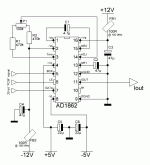
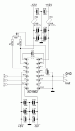
I've attached the schematic. This is the actual circuit I'm listening to as we speak. I've made it on a prototype board with ground plane.
As for the MSB-trim I know Jocko Homo believes that it's mandatory, and he has a lot of experience with this chip. I get noise on the output when applying a -60dB test tone into the dac, with the amplifier at full level into 110 dB sensitive level. With the trim circuit I managed to adjust it until the noise disappeared. So I'd like to keep the trim option in the design.
I tried to locate the thread on this forum where someone had measured a lot of different coupling cap combinations, showing a lot of the common bypass arrangements creating a huge impedance peak at high frequencies. I only found this thread for now: http://www.diyaudio.com/forums/power-supplies/106648-paralleling-film-caps-electrolytic-caps.html#post1276060 I believe it might be relevant as well. I'll continue to search for the measurements, and post them when i find them.
I understand the idea of partitioning the PCB into digital and analog sections. This is super easy for the PCM63 and the AD1865 with their interiors split at the middle. But the AD1862 seems to have something like a quarter of the interiors for the digital parts, which makes it harder to position the chips on the PCB, since it's a mono chip and you's need at least two chips.
I've attached the schematic. This is the actual circuit I'm listening to as we speak. I've made it on a prototype board with ground plane.
As for the MSB-trim I know Jocko Homo believes that it's mandatory, and he has a lot of experience with this chip. I get noise on the output when applying a -60dB test tone into the dac, with the amplifier at full level into 110 dB sensitive level. With the trim circuit I managed to adjust it until the noise disappeared. So I'd like to keep the trim option in the design.
Attachments
Slightly different to decoupling on PCBs, especially digital IC's, the PCB parasitics damp these resonances, as does using MLCC X7R decoupler's for the local caps.
Got to go for my train now so I'll be off line for a while 45hrs travel, no internet, I shall get back tomorrow.
Got to go for my train now so I'll be off line for a while 45hrs travel, no internet, I shall get back tomorrow.
Slightly different to decoupling on PCBs, especially digital IC's, the PCB parasitics damp these resonances, as does using MLCC X7R decoupler's for the local caps.
Got to go for my train now so I'll be off line for a while 45hrs travel, no internet, I shall get back tomorrow.
So putting 100 nF SMD ceramics as close to the pins as possible will be the way to go. At least for the digital line.
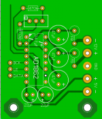
By the way, I've put a ground layer on the top of the board. All traces are on the bottom. So in the picture I provided in the first post the light green is the top ground plane layer, and the dark green traces are on the bottom layer.
painkiller,
Do you want to make two mono DAC with a common I2S ?
Well, I would like to have it all on one board. Two dacs, IV-stages and power supply. That is if I can solve the digital/analog ground issue. If I interpret the datasheet correctly the interior of the AD1862 is not split in half like most other chips, so with two chips placed beside each other the digital line on one of the dacs will create noise on the analog ground on the other chip. That's part of why I've come here for help.
Routing a two layer board is much easier with only one dac per board. But two dacs on one board would be preferred.
And, yes, there will be only one I2S signal for the two dac chips. They have to share the latch enable and bitclock, while the data lines are separate for each dac. I use Iancanada's "I2S to PCM converter".
Yes 0.1uF next to the pins is and always has been done for decoupling both analogue and digital devices for as long as I have been laying out PCBs (28 years).
There is a big difference to decoupling electrolytic smoothing capacitors, and is shown on all data sheets for IC's or in the layout or decoupling app notes, usually separate for larger devices such as FPGAs
There is a big difference to decoupling electrolytic smoothing capacitors, and is shown on all data sheets for IC's or in the layout or decoupling app notes, usually separate for larger devices such as FPGAs
I added 100 nF X7R decoupling caps on all supply lines. Seems to work very well. Sounds better than my previous AD1865 dac.
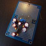
I've attached a couple photos of the prototype board. I put the trim circuit underneath the board. As per the schematic, the caps are 22uF and 47uF (Elna Cerafine).
I've attached a couple photos of the prototype board. I put the trim circuit underneath the board. As per the schematic, the caps are 22uF and 47uF (Elna Cerafine).
Attachments
I am commuting down to London during the week and spend 9-11 hours travelling a weekend so must apologise as I haven't had as much spare time lately, I have done some playing about and when I get chance will reply in more detail....
A four layer design will always give you more choices and generally a better layout, plus shielding form EMC.
Back soon, I haven't forgotten
A four layer design will always give you more choices and generally a better layout, plus shielding form EMC.
Back soon, I haven't forgotten
That sounds exhausting. Your help is much appreciated.
I've attached another schematic. I noticed that "hott" recommended using 2 x 100nF per rail, so I put that in there.
I've been playing around a bit myself, with routing a four layer board. It'll be interresting to see your take on it as well.
I've attached another schematic. I noticed that "hott" recommended using 2 x 100nF per rail, so I put that in there.
I've been playing around a bit myself, with routing a four layer board. It'll be interresting to see your take on it as well.
Attachments
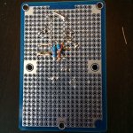
This is more or less how I interpret the internals of the dac. The pinout of the AD1865 (to the right) shows that the dacs internal digital and analog circuitry is neatly separated along the middle. So placing two dacs beside each other is no problem. Partitioning of the board into analog and digital grounds is easy.
With the AD1862 I get confused. How do you position two chips on one board without mixing up the analog and digital grounds?
With the AD1862 I get confused. How do you position two chips on one board without mixing up the analog and digital grounds?
Attachments
Do you mean, there is already an common ground between the two digital & analog in the chip and you want avoid a ground loop by using two pcb: one for digital, one for analog, the dac chip on the both with a space between the two (shown in red on your picture)?
Is your verroboard with contigous plane beneath it, I understand it is on the picture ?
If one contigous ground beneath the verroboard is used : Could an horizontal trace without copper (you get of the copper yourself) at the position shown in red in your picture work ? For example a cut long enough : 2 cm longer to each side of the chip : so a 6 cm trace...
What do you use here ? And plan to do ?
Thank you
Last edited:
Do you mean, there is already an common ground between the two digital & analog in the chip and you want avoid a ground loop by using two pcb: one for digital, one for analog, the dac chip on the both with a space between the two (shown in red on your picture)?
Is your verroboard with contigous plane beneath it, I understand it is on the picture ?
I'll try to clarify what I mean.
I want to make a PCB with only one ground plane. DGND and AGND will share the same ground plane, but the analog and digital loops should be separated on the board. Partitioned instead of split ground.
And since the AD1862 is a mono dac chip, you'd need two of them. I have to find out how to best position the chips on the PCB in order not to mix up the ground current loops.
- Home
- Source & Line
- Digital Line Level
- AD1862 PCB layout