OK. I am unable to model -6.2mA on both the + and - pins of the current generator in Tina. So, I just modeled this part of the schematic and set the generator to 7.8mA sine wave with a -6.2mA DC offset. Performance is very good but there's a DC offset of -1.55V on the output. I don't know if that's a big deal. Distortion, noise and bandwidth are all excellent. S/N is 140dB. I'm impressed. The NE5534 performs extremely well. Input noise is 13picoV/Hz^0.5. Gain is just right at about 50dB. Of course, I adjusted the feedback resistor to achieve that. It seems to be fine at low resistor values. The outputs are running at 23mA. I didn't spend much time optimizing it.
Attachments
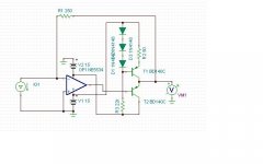
OK. I am unable to model -6.2mA on both the + and - pins of the current generator in Tina. So, I just modeled this part of the schematic and set the generator to 7.8mA sine wave with a -6.2mA DC offset. Performance is very good but there's a DC offset of -1.55V on the output
Dirk,
That -1.55V offset is due to the -6.2mA bias current, and is correct for the the 250R feedback resistor used in your circuit. -6.2mA x 250R = -1.55V. No matter what value feedback resistor you use there will be a negative output voltage offset generated by the -6.2mA bias current. Which means that this circuit, as is, cannot be D.C. coupled and will require an output coupling cap.
You could implement a D.C. servo, which would need sink the entire -6.2mA bias current directly at the DAC's output pin. The main issue I foresee there is that the servo output would likely not have a very high output impedance, which means that it might contribute distortion to the signal. A more elegant solution for D.C. coupling would be to have an 6.2mA active current-sink (such as a JFET or an LM334) attached to the DAC's output pin, but obtaining zero would require manual adjustment. These solutions would require implementing a negative power supply.
Last edited:
Dirk,
That -1.55V offset is due to the -6.2mA bias current, and is correct for the the 250R feedback resistor used in your circuit. -6.2mA x 250R = -1.55V. No matter what value feedback resistor you use there will be a negative output voltage offset generated by the -6.2mA bias current. Which means that this circuit, as is, cannot be D.C. coupled and will require an output coupling cap.
You could implement a D.C. servo, which would need sink the entire -6.2mA bias current directly at the DAC's output pin. The main issue I foresee there is that the servo output would likely not have a very high output impedance, which means that it might contribute distortion to the signal. A more elegant solution for D.C. coupling would be to have an 6.2mA active current-sink (such as a JFET or an LM334) attached to the DAC's output pin, but obtaining zero would require manual adjustment. These solutions would require implementing a negative power supply.
Thanks Ken, I appreciate your comments. What I modeled was only part of the entire TI circuit, since Tina doesn't allow me to have 2 signal sources in the same circuit, and I can't model -6.2mA on both pins of a single current source. What's missing from the circuit I posted is another IV converter identical to this one, and a balanced-to-unbalanced following opamp. I don't know what will be the result of -1.55V on both the + and - pins of the following opamp, mostly because I can't figure that out in my head. I guess it won't be a big deal but I can't do the math in my head. I was asked to model simms73's circuit earlier (post #3) and I finally got around to it now. I have software limitations that prevent me from modeling the entire TI circuit.
Use a separate CCS to model the 6.2mA center current.
Use IG to model the 7.8mA signal current.
Maybe that will work.
Use IG to model the 7.8mA signal current.
Maybe that will work.
OK. I am unable to model -6.2mA on both the + and - pins of the current generator in Tina. So, I just modeled this part of the schematic and set the generator to 7.8mA sine wave with a -6.2mA DC offset. Performance is very good but there's a DC offset of -1.55V on the output. I don't know if that's a big deal. Distortion, noise and bandwidth are all excellent. S/N is 140dB. I'm impressed. The NE5534 performs extremely well. Input noise is 13picoV/Hz^0.5. Gain is just right at about 50dB. Of course, I adjusted the feedback resistor to achieve that. It seems to be fine at low resistor values. The outputs are running at 23mA. I didn't spend much time optimizing it.
Use a separate CCS to model the 6.2mA center current.
Use IG to model the 7.8mA signal current.
Maybe that will work.
I think I tried something like that and the software got confused, or I got strange results. I can try again, thanks for the suggestion.
I have been trying to follow this thread and learn more about I/V and just want to make sure I am getting my facts straight.
The Iout+ on pcm1794 put out between -2.3mA and -10.1mA centered on -6.2mA.
The Iout- put out between -2.3mA and -10.1mA 180 degrees out of phase with the Iout+ pins.
Is that correct?
The Iout+ on pcm1794 put out between -2.3mA and -10.1mA centered on -6.2mA.
The Iout- put out between -2.3mA and -10.1mA 180 degrees out of phase with the Iout+ pins.
Is that correct?
I have been trying to follow this thread and learn more about I/V and just want to make sure I am getting my facts straight.
The Iout+ on pcm1794 put out between -2.3mA and -10.1mA centered on -6.2mA.
The Iout- put out between -2.3mA and -10.1mA 180 degrees out of phase with the Iout+ pins.
Is that correct?
Yup.
Dirk, you can try to put a 220 Ohm resistor between base and emitter of T2. Has nothing to do with the offset.
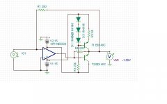
Did I do it right? Doesn't seem to make a difference.
Attachments
You correctly injected the current into the NE from the positive side. It is a idiosyncrasy of the NE5534. Good PNP where not available at that time for the output buffer. With this trick the NE performs as good as the best Opamps on the market in many ways. Mind over matter.
You correctly injected the current into the NE from the positive side. It is a idiosyncrasy of the NE5534. Good PNP where not available at that time for the output buffer. With this trick the NE performs as good as the best Opamps on the market in many ways. Mind over matter.
OK, thanks. THD is 8.7x10^-6% and S/N is -140dB (@1 kHz) for output of 2.07Vrms. Looks like a winner to me.
Obviously, input impedance is extremely low as well.
dirkwright said:What's missing from the circuit I posted is another IV converter identical to this one, and a balanced-to-unbalanced following opamp. I don't know what will be the result of -1.55V on both the + and - pins of the following opamp, mostly because I can't figure that out in my head. I guess it won't be a big deal but I can't do the math in my head.
Such a bal-to-unbal. op-amp would reject the -1.55V applied to both input pins since they would represent a common-mode voltage. If the input offset voltages are identical, the output of the bal-to-unbal. op-amp would be zero volts with respect to ground. If there is a small D.C. difference between the two input offset voltsges, which there likely would be, that difference will be multiplied by the closed-loop gain of the bal-to-unbal. op-amp. For example, if the input offset difference was 10mV, and the closed-loop gain of the bal-to-unbal. op-amp was 2, then the D.C. offset at the ouput of the bal-to-unbal. op-amp would be 20mV, plus the intrinsic D.C. offset of this op-amp.
Last edited:
Such a bal-to-unbal. op-amp would reject the -1.55V applied to both input pins since they would represent a common-mode voltage. If the input offset voltages are identical, the output of the bal-to-unbal. op-amp would be zero volts with respect to ground. If there is a small D.C. difference between the two input offset voltsges, which there likely would be, that difference will be multiplied by the closed-loop gain of the bal-to-unbal. op-amp. For example, if the input offset difference was 10mV, and the closed-loop gain of the bal-to-unbal. op-amp was 2, then the D.C. offset at the ouput of the bal-to-unbal. op-amp would be 20mV, plus the intrinsic D.C. offset of this op-amp.
OK, thank you again. That makes sense.
The OPA1641 should work too. I think it has a GB of 10MHz.
Yes it will work.
I have been simulating the phase of the buffers. And it is only 6° at 100 Mhz with BC550c or 2n3904 with BC327 is 15° .is less than 1° at 10Mhz. This is much better than I expected.
Dirk, you can try to put a 220 Ohm resistor between base and emitter of T2. Has nothing to do with the offset.
There is no need to use this trick in this circuit. As the buffers have a high input impedance and the NE5534 will always stay in class A .
Joachim don't you think is better to use a current source in replace for the 220 ohms ?
Last edited:
It is a idiosyncrasy of the NE5534. Good PNP where not available at that time for the output buffer
Unfortunately even today the npn transistors are better than the pnp.
- Status
- This old topic is closed. If you want to reopen this topic, contact a moderator using the "Report Post" button.
- Home
- Source & Line
- Digital Source
- The pcm1794a datasheet I/V converter and how to improve it.