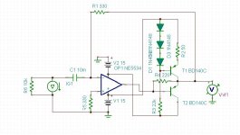
This is what I suggest. Block the DC at the input and balance the input and feedback resistors so that the DC offset at the output will be 16uV, which is insignificant. Noise is still good with S/N near 140dB. AC response is flat from 1Hz to infinity apparently. It's just a flat line. THD is extremely low. After looking at the schematic for the NE5534, I realized that I'd played around with discrete opamps before, and so I realized that it's incorrect to just tie one of the input bases to ground. There needs to be a resistor there that is equal to the feedback resistor. Also, I have realized that a blocking capacitor is necessary for good DC balance in the circuit. I have further realized that when the DC balanced is achieved, then the opamp performs better. So, this is what I came up with now.
Actually, this may not work with the DAC because it appears to want a DC path to ground. I'm not sure of that now. Why would the DAC need a DC path to ground? I know I read about it in some application notes, but I don't see why this would not work. We're only interested in the AC signal after all.
As for my discrete IV converter, I have not done anything more with it. I'm trying to find the problem with a power supply a built, and I'm building Pete Millett's sound card interface and hoping to buy the PCM4222 ADC soon. I need good test gear before getting serious about building stuff.
Attachments
Last edited:
If a DC path is needed we have discussed the option to insert an opposing current directly into the output of the DAC with a J-Fet CCS.
Yeah, I don't understand right now why a DC is needed at all. They say it in the various application notes, but what would happen if there wasn't one? We're interested in an AC current after all, not a DC one.
I can not tell. The only experience i have in years with DACs myself is the new ESS with voltage output. I designed a buffer for them but that is all. There is a guy on this forum, his avatar is Calvin. He seems to know all about that.
I am planning though to build a DAC so i am contributing here a bit and watch what you and our friend from Portugal is coming up with.
I am planning though to build a DAC so i am contributing here a bit and watch what you and our friend from Portugal is coming up with.
Maybe you put it in to get rid of a peak.
The capacitor is necessary. Without it the DC offset on the output is 11 volts!
In the original schematic, there was just a capacitor between the transformer + and ground. I found I needed a huge capacitor to get good response with low feedback resistors and there was still a nasty peak. I reduced the capacitor and added the resistor to dampen the response, which is now nice and smooth down to about 1Hz. The bad news is that the 75 ohm resistor adds to the input impedance as seen by the current generator. I think it's about 50 ohms or so. Still, this DAC seems to be OK with higher than zero load impedances.
The circuit is just a variation of the single opamp balanced to unbalanced converter, where the first resistor on the - pin is replaced by the transformer secondary winding. I don't know why the capacitor is required. So, R3 has to be set to the DC resistance of the transformer secondary and R1 and R2 have to be equal.
Well, the other circuit I developed that has the current mirrors is still better in terms of low noise compared to these circuits I'm playing with that use chips. The distortion may not be as low, but I think it's probably low enough. I've tried all kinds of variations on these chip circuits and did not come up with anything really good.
I think that with the buffers we can have both low distortion and low noise.
what you guys think? and what is your experience.
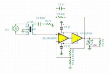
I think the BUF634 is good enough, and easy enough to use, but if one wanted to go "whole hog", then an SMD implementation with the LME49990 + LME49600 would be the way to go for each "super op amp". I'm going with something much easier though; the LME49710 + BUF634 in 8 pin dip form and through hole devices.
Dear All,
Very nice and informative thread.
Once again the NE5534 shows up. And those who mentioned to use pin5 and feed a buffer with that are very right! That is the way to go, and one of the best NE5534's secrets.
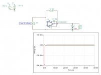
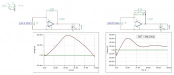
The NE5534 is often cursed as the "bad" Op Amp. However I would like to show you some some simulations in Tina, How the NE5534 actually deals better with glitches and fast pulses then more expensive types.
You can try two approaches. 1, To avoid/filter out the fast rising glitches of the DAC completely. Or 2, Let the I-V converter follow those steps as accurate as possible. (Or of course a combination of both)
See the simulations below. The current generator is set on a 1nS, 3,9mA PP Pulse.
IV TEST1: Shows the NE5534 with 100p miller compensation. As you can see it follows the pulse very accurate.
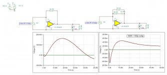
IV TEST2: Shows the OPA627 with feedback compensation and without. With compensation we can filter out the glitch to round 50mV at it's peak.
IV TEST3: Shows the AD797 with feedback compensation and without. With compensation we can filter out the glitch to round 60mV at it's peak.
Pick your poison....
Of course this are just simulations with many variables and errors possible. But based on that alone I would prefer the NE5534 as I-V convertor. TI isn't so silly after all for explicit choosing this Op Amp for IV duties in their high-end DAC.
Secondly, unlike most Op Amps, the NE5534 is designed to drive impedances as low as 600 Ohms. So even without buffer, it would be able to deal better with the low impedance input from the following lowpass filter/instrumentation amplifier. I think this is another reason why TI picked to NE5534 on this occasion.
One question for those who work with Tina. Why is it that when I set the current source value on e.g. 7.8mA PP that I don't get a differential 7.8ma PP? I should get 3.9mA PP in opposite phase on each leg of the current source.... But I don't. I get 7.8mA PP on each leg.
With kind regards,
Bas
Very nice and informative thread.
Once again the NE5534 shows up. And those who mentioned to use pin5 and feed a buffer with that are very right! That is the way to go, and one of the best NE5534's secrets.
The NE5534 is often cursed as the "bad" Op Amp. However I would like to show you some some simulations in Tina, How the NE5534 actually deals better with glitches and fast pulses then more expensive types.
You can try two approaches. 1, To avoid/filter out the fast rising glitches of the DAC completely. Or 2, Let the I-V converter follow those steps as accurate as possible. (Or of course a combination of both)
See the simulations below. The current generator is set on a 1nS, 3,9mA PP Pulse.
IV TEST1: Shows the NE5534 with 100p miller compensation. As you can see it follows the pulse very accurate.
IV TEST2: Shows the OPA627 with feedback compensation and without. With compensation we can filter out the glitch to round 50mV at it's peak.
IV TEST3: Shows the AD797 with feedback compensation and without. With compensation we can filter out the glitch to round 60mV at it's peak.
Pick your poison....
Of course this are just simulations with many variables and errors possible. But based on that alone I would prefer the NE5534 as I-V convertor. TI isn't so silly after all for explicit choosing this Op Amp for IV duties in their high-end DAC.
Secondly, unlike most Op Amps, the NE5534 is designed to drive impedances as low as 600 Ohms. So even without buffer, it would be able to deal better with the low impedance input from the following lowpass filter/instrumentation amplifier. I think this is another reason why TI picked to NE5534 on this occasion.
One question for those who work with Tina. Why is it that when I set the current source value on e.g. 7.8mA PP that I don't get a differential 7.8ma PP? I should get 3.9mA PP in opposite phase on each leg of the current source.... But I don't. I get 7.8mA PP on each leg.
With kind regards,
Bas
Attachments
Last edited:
Hi Bas,
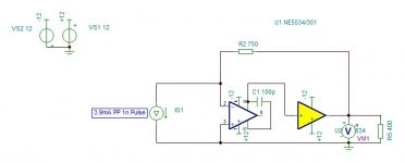
What model are you using? Macromodel or transistor level or something in between? Your plot for the 5534 simulation shows a 200mV step in well under 1nS - that's a slew rate of >1V/5nS or better than 200V/uS. How can this come out of an overcompensated 5534 which only gets 13V/uS with no comp cap?
Curious how TI's application doesn't look much like your schematic - from what I recall they have something like 2n2 across the feedback resistor, no 100pF comp cap.
IV TEST1: Shows the NE5534 with 100p miller compensation. As you can see it follows the pulse very accurate.
What model are you using? Macromodel or transistor level or something in between? Your plot for the 5534 simulation shows a 200mV step in well under 1nS - that's a slew rate of >1V/5nS or better than 200V/uS. How can this come out of an overcompensated 5534 which only gets 13V/uS with no comp cap?
Of course this are just simulations with many variables and errors possible. But based on that alone I would prefer the NE5534 as I-V convertor. TI isn't so silly after all for explicit choosing this Op Amp for IV duties in their high-end DAC.
Curious how TI's application doesn't look much like your schematic - from what I recall they have something like 2n2 across the feedback resistor, no 100pF comp cap.
Hi Abraxalito,
Good to hear from you! I hope everything is okay your side. My sincere apologies our contact got cut off. I have bin sick for a long time. However I am active again as you can see
This is the Macro model I used in Tina. Me too think it is an error in the model. However Consistently I get amazing results with the NE5534 in simulations.
This is the Macro:
*
* NE5534/301 OPERATIONAL AMPLIFIER "MACROMODEL" SUBCIRCUIT
* CREATED USING PARTS RELEASE 4.01 ON 04/10/89 AT 12:41
* (REV N/A) SUPPLY VOLTAGE: +/-15V
* CONNECTIONS: NON-INVERTING INPUT
* | INVERTING INPUT
* | | POSITIVE POWER SUPPLY
* | | | NEGATIVE POWER SUPPLY
* | | | | OUTPUT
* | | | | | COMPENSATION
* | | | | | / \
.SUBCKT NE5534/301 1 2 3 4 5 6 7
*
C1 11 12 7.703E-12
DC 5 53 DX
DE 54 5 DX
DLP 90 91 DX
DLN 92 90 DX
DP 4 3 DX
EGND 99 0 POLY(2) (3,0) (4,0) 0 .5 .5
FB 7 99 POLY(5) VB VC VE VLP VLN 0 2.893E6 -3E6 3E6 3E6 -3E6
GA 6 0 11 12 1.382E-3
GCM 0 6 10 99 13.82E-9
IEE 10 4 DC 133.0E-6
HLIM 90 0 VLIM 1K
Q1 11 2 13 QX
Q2 12 1 14 QX
R2 6 9 100.0E3
RC1 3 11 723.3
RC2 3 12 723.3
RE1 13 10 329
RE2 14 10 329
REE 10 99 1.504E6
RO1 8 5 50
RO2 7 99 25
RP 3 4 7.757E3
VB 9 0 DC 0
VC 3 53 DC 2.700
VE 54 4 DC 2.700
VLIM 7 8 DC 0
VLP 91 0 DC 38
VLN 0 92 DC 38
.MODEL DX D(IS=800.0E-18)
.MODEL QX NPN(IS=800.0E-18 BF=132)
.ENDS
With kind regards,
Bas
Hi Bas,
What model are you using? Macromodel or transistor level or something in between? Your plot for the 5534 simulation shows a 200mV step in well under 1nS - that's a slew rate of >1V/5nS or better than 200V/uS. How can this come out of an overcompensated 5534 which only gets 13V/uS with no comp cap?
Curious how TI's application doesn't look much like your schematic - from what I recall they have something like 2n2 across the feedback resistor, no 100pF comp cap.
I think there's something wrong with the spice model of the NE5534 in Tina because the first circuit doesn't perform very well at all whereas the second one is outstanding. I see from the schematic of the actual chip that it does make sense to take the output from pin 5, but the spice model appears to be different.
Attachments
I think there's something wrong with the spice model of the NE5534 in Tina because the first circuit doesn't perform very well at all whereas the second one is outstanding. I see from the schematic of the actual chip that it does make sense to take the output from pin 5, but the spice model appears to be different.
Dear dirkwright,
There is an error in the spice model of the NE5534. Pin 5 out is pin 8 in the spice model. Then it works
So with other words, if you connect pin 8 to the buffer (instead of the actual output) then it works.
I think there's something wrong with the spice model of the NE5534 in Tina because the first circuit doesn't perform very well at all whereas the second one is outstanding. I see from the schematic of the actual chip that it does make sense to take the output from pin 5, but the spice model appears to be different.
Like this:
Attachments
Good to hear from you! I hope everything is okay your side. My sincere apologies our contact got cut off. I have bin sick for a long time. However I am active again as you can see
Indeed its a pleasure to see you back and I hope your health has fully recovered now
Everything's going swimmingly over on my side, getting some very pleasing sounds out of my latest DAC incarnation.I looked at your listing but its too impenetrable to me. My ability to read Spice netlists is poor. It looks like a kind of hybrid model with some transistors but certainly a long way from the full complement of the chip. Perhaps you could develop your own based on the very helpful paper by Alexander and Bowers. If you can't find it I could get the link for you. I could also send you my model for the LM1876 based on their template which wouldn't be too difficult to modify to the NE5534. There is one thing about the 5534 though which requires a bit of attention - there's some lead-lag compensation going on, shown by a kink in the phase curve.
Like this:
OK, but performance is not better as far as I can see. Thanks for the tip though.
- Status
- This old topic is closed. If you want to reopen this topic, contact a moderator using the "Report Post" button.
- Home
- Source & Line
- Digital Source
- The pcm1794a datasheet I/V converter and how to improve it.