In the thread “Zen -> Cen -> Sen, evolution of a minimalistic IV Converter” and in an article in Linear Audio Vol. 2, EUVL has given us an IV converter for “current-output” DACs. Acknowledged as inspired by a MC-step-up preamp stage by the late Marshall Leach, which used bipolar transistors, the EUVL stage uses JFETs. The distinctive feature inherited from the Leach circuit is the use of a floating power supply.
The performance of the simple circuit is quite good considering its simplicity. However, the distortion performance degrades when the DAC output impedance is smaller than the 20k resistor used for the published tests.
There are two issues here. The less-serious one is probably the DAC behavior itself: terminating the signal in a nonzero impedance can create errors in the output current that are code-dependent. Some manufacturers in fact specify the maximum voltage swing permissible to preserve the stated accuracy. However, the circuit presented, with two parallel common-gate 2SK170 devices and associated matched current sources, manages about 15 ohms, which for the roughly 1k || 22pF output impedance of the selected DAC is probably low enough to cause negligible errors.
The second issue comes up when we consider the variation in that 15 ohms with current, which although small is still significant as a distortion mechanism. The other sources of distortion for the stage include the variation in drain-gate capacitances of the JFETs, and these become progressively more important at higher frequencies.
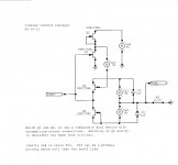
Addressing the input resistance variations, I have explored a “repurposing” of the JFETs in a novel fashion, in which two of them are used to make an amplifier with high negative gain. An additional power supply, which is referenced to circuit common, powers the new stage, which consists of a common-source JFET loaded by a matched JFET current source. A floating offset voltage from the lower JFET drain, which can be provided by a primary battery (there is negligible current flowing) couples the amplifier output to the gate of the now- single conveyor input device, and the amplifier input gate is connected to the conveyor input. I’ve shown the floating supply as center-tapped, and the whole circuit d.c.-coupled, as noise measurements of NiMH batteries have been encouraging, but a mostly-a.c.-coupled arrangement similar to the Sen circuit can also be used. The 1uF capacitors should be used to remove some high-frequency peaking that is associated with battery pack parasitics.
The circuit is predicted to have exemplary distortion performance, with the residual effects mostly due to the mentioned capacitance variations. Cascode structures used with a higher voltage supply can greatly reduce those effects, but for the moment it’s interesting to see how little effort it takes to get this far.
Note as well that the noise performance is now almost wholly dependent on the equivalent input noise of the amplifier, which for 2SK170 devices run at Idss is of order 800pV/sqrtHz; the use of a second similar device as the load raises this by 3dB. So we can anticipate e sub n as about 1.13nV/sqrtHz, and the effect when terminated with the 1k DAC output resistance as a noise current passed to the circuit output of 1.13pA/sqrtHz. This is small compared to the noise of the DAC, or even of a physical 1k resistor (4.07pA/sqrtHz at 300 K). The output termination resistor will determine the unloaded output noise. In any event, although there are ways to further reduce the amplifier noise, there is little motivation in this example.
Note that the matching requirements on the input devices are reduced in this circuit, since the input offset voltage is almost entirely a function of the amplifier offset. Moreover, the input impedance is greatly reduced, and for the anticipated 1mA rms the excursion at the common-gate ( or driven-gate) stage at the peak current of -1.414mA is only about 52mV --- thus, we are still far away from any significant forward-biased gate conduction. And this is with only one input device. The circuit input impedance is modeled closely up to well above the highest audio frequencies as 83 milliohms in series with a 563 nH inductance, when driven from the assumed 1k source and terminated in the Sen 2.7k resistor. Before capacitive loading of that resistor, the frequency response is free from peaking and -3dBr at about 11.6MHz. Of course the response can be tailored by a parallel capacitor as well as cable capacitance, or a suitable buffer provided.
The power supply rejection for the floating supplies is also very good. For the suggested 6V grounded supply it’s desirable that the exact voltage be twice that of the floating 3V supply. One way to do this is to provide a regulator whose reference voltage is a battery of similar type to the 3V battery, since the two will tend to track with temperature.
Another advantage to this approach can be appreciated when other DACs with unipolar output currents are considered. Because the input resistance of this conveyor is low and stable, a simple resistor to a stable voltage can provide the necessary offsetting current. The only penalty is a small increase in noise due to the further reduction of equivalent source resistance. Although a current source would remove this, the noise of it would in most cases exceed any increase in noise due to the envisaged resistor, provided the associated voltage source is not too low.
The distortion performance predicted from simulations: at 1kHz, 1mA rms, harmonics to 9th, 11.1ppm dominated by second (third is -115dB); at 10kHz, 1mA rms, harmonics to 5th, 110ppm. The Sen without the amplifier but with two pairs of JFETs is predicted, with the 1k source impedance, to produce 101ppm under the same drive at 1kHz, and at 10kHz, 227ppm. The smaller improvement at 10kHz is indicative of the input distortion becoming less important compared to the JFET capacitance-variation distortion mechanism, and as remarked this latter can be drastically reduced with cascode structures. Bandwidth is also extended, and some compensation is required to reduce output response peaking. It also helps to make the amplifier section a cascode arrangement. But that’s a subject for another thread.
A very tight layout is advised to reduce parasitic inductances, and there nonetheless may be a need to damp same with small-value resistors or ferrites to tame VHF oscillations.
The performance of the simple circuit is quite good considering its simplicity. However, the distortion performance degrades when the DAC output impedance is smaller than the 20k resistor used for the published tests.
There are two issues here. The less-serious one is probably the DAC behavior itself: terminating the signal in a nonzero impedance can create errors in the output current that are code-dependent. Some manufacturers in fact specify the maximum voltage swing permissible to preserve the stated accuracy. However, the circuit presented, with two parallel common-gate 2SK170 devices and associated matched current sources, manages about 15 ohms, which for the roughly 1k || 22pF output impedance of the selected DAC is probably low enough to cause negligible errors.
The second issue comes up when we consider the variation in that 15 ohms with current, which although small is still significant as a distortion mechanism. The other sources of distortion for the stage include the variation in drain-gate capacitances of the JFETs, and these become progressively more important at higher frequencies.
Addressing the input resistance variations, I have explored a “repurposing” of the JFETs in a novel fashion, in which two of them are used to make an amplifier with high negative gain. An additional power supply, which is referenced to circuit common, powers the new stage, which consists of a common-source JFET loaded by a matched JFET current source. A floating offset voltage from the lower JFET drain, which can be provided by a primary battery (there is negligible current flowing) couples the amplifier output to the gate of the now- single conveyor input device, and the amplifier input gate is connected to the conveyor input. I’ve shown the floating supply as center-tapped, and the whole circuit d.c.-coupled, as noise measurements of NiMH batteries have been encouraging, but a mostly-a.c.-coupled arrangement similar to the Sen circuit can also be used. The 1uF capacitors should be used to remove some high-frequency peaking that is associated with battery pack parasitics.
The circuit is predicted to have exemplary distortion performance, with the residual effects mostly due to the mentioned capacitance variations. Cascode structures used with a higher voltage supply can greatly reduce those effects, but for the moment it’s interesting to see how little effort it takes to get this far.
Note as well that the noise performance is now almost wholly dependent on the equivalent input noise of the amplifier, which for 2SK170 devices run at Idss is of order 800pV/sqrtHz; the use of a second similar device as the load raises this by 3dB. So we can anticipate e sub n as about 1.13nV/sqrtHz, and the effect when terminated with the 1k DAC output resistance as a noise current passed to the circuit output of 1.13pA/sqrtHz. This is small compared to the noise of the DAC, or even of a physical 1k resistor (4.07pA/sqrtHz at 300 K). The output termination resistor will determine the unloaded output noise. In any event, although there are ways to further reduce the amplifier noise, there is little motivation in this example.
Note that the matching requirements on the input devices are reduced in this circuit, since the input offset voltage is almost entirely a function of the amplifier offset. Moreover, the input impedance is greatly reduced, and for the anticipated 1mA rms the excursion at the common-gate ( or driven-gate) stage at the peak current of -1.414mA is only about 52mV --- thus, we are still far away from any significant forward-biased gate conduction. And this is with only one input device. The circuit input impedance is modeled closely up to well above the highest audio frequencies as 83 milliohms in series with a 563 nH inductance, when driven from the assumed 1k source and terminated in the Sen 2.7k resistor. Before capacitive loading of that resistor, the frequency response is free from peaking and -3dBr at about 11.6MHz. Of course the response can be tailored by a parallel capacitor as well as cable capacitance, or a suitable buffer provided.
The power supply rejection for the floating supplies is also very good. For the suggested 6V grounded supply it’s desirable that the exact voltage be twice that of the floating 3V supply. One way to do this is to provide a regulator whose reference voltage is a battery of similar type to the 3V battery, since the two will tend to track with temperature.
Another advantage to this approach can be appreciated when other DACs with unipolar output currents are considered. Because the input resistance of this conveyor is low and stable, a simple resistor to a stable voltage can provide the necessary offsetting current. The only penalty is a small increase in noise due to the further reduction of equivalent source resistance. Although a current source would remove this, the noise of it would in most cases exceed any increase in noise due to the envisaged resistor, provided the associated voltage source is not too low.
The distortion performance predicted from simulations: at 1kHz, 1mA rms, harmonics to 9th, 11.1ppm dominated by second (third is -115dB); at 10kHz, 1mA rms, harmonics to 5th, 110ppm. The Sen without the amplifier but with two pairs of JFETs is predicted, with the 1k source impedance, to produce 101ppm under the same drive at 1kHz, and at 10kHz, 227ppm. The smaller improvement at 10kHz is indicative of the input distortion becoming less important compared to the JFET capacitance-variation distortion mechanism, and as remarked this latter can be drastically reduced with cascode structures. Bandwidth is also extended, and some compensation is required to reduce output response peaking. It also helps to make the amplifier section a cascode arrangement. But that’s a subject for another thread.
A very tight layout is advised to reduce parasitic inductances, and there nonetheless may be a need to damp same with small-value resistors or ferrites to tame VHF oscillations.
Attachments
Allow me a stupid question :
> the input impedance is greatly reduced, and for the anticipated 1mA rms the excursion at the common-gate ( or driven-gate) stage at the peak current of -1.414mA is only about 52mV
Does that not work out to be 36.8R Zin ?
Patrick
No, that is the voltage swing on the gate of Q3. At the source it is tiny, in keeping with the stated low input impedance.
I'm getting almost 70dB of gain. Is that correct? There's also a 6dB peak at about 150kHz in the response. THD is about 0.001% (if I delay the FFT by 40usec). S/N is about 110dB @ 1kHz.
70dB of gain where?
My model shows no peaking in the response at all, just flat with a smooth rolloff such that the response is -3dB at about 12MHz.
70dB of gain where?
My model shows no peaking in the response at all, just flat with a smooth rolloff such that the response is -3dB at about 12MHz.
Well, measured at the output.
Maybe the differences are due to the difference spice models I'm using. I don't know, I'm just trying to be helpful.
Allow me a stupid question :
> the input impedance is greatly reduced, and for the anticipated 1mA rms the excursion at the common-gate ( or driven-gate) stage at the peak current of -1.414mA is only about 52mV
Does that not work out to be 36.8R Zin ?
Patrick
I measure a very low input impedance in the sim. It's less than 1 ohm.
Attachments
Hi,
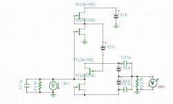
I used the LSK389Cco model and LTSpice4.
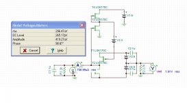
With an input amplitude of +-1mA (1k ||22pF) the results I got are:
V(out): 1.909Vrms
Fourier components of V(out)
DC component:-2.50803e-006
Harmonic Frequency Fourier Normalized Phase Normalized
Number [Hz] Component Component [degree] Phase [deg]
1 1.000e+03 2.700e+00 1.000e+00 179.98° 0.00°
2 2.000e+03 5.670e-05 2.100e-05 2.45° -177.53°
3 3.000e+03 6.035e-06 2.236e-06 -91.06° -271.05°
4 4.000e+03 6.834e-07 2.531e-07 -179.91° -359.89°
Total Harmonic Distortion: 0.002112% -93.5dB
The input impedance stays around 90mR 0° up to app. 10kHz (140mR 49°), than starts rising (1R @100kHz 82°), eventually peaking (68R @175MHz 1°), then dropping again. Besides the rise in impedance the early and strong shift of phase looks troublesome.
F-3dB: 3.6MHz
Noise (20-20k): 1.8535µV -114.6dBV
Actually apart from the generally lower imput impedance value I don´t see an improvement over the simpler SEN, but rather worse behaviour.
jauu
Calvin
I used the LSK389Cco model and LTSpice4.
With an input amplitude of +-1mA (1k ||22pF) the results I got are:
V(out): 1.909Vrms
Fourier components of V(out)
DC component:-2.50803e-006
Harmonic Frequency Fourier Normalized Phase Normalized
Number [Hz] Component Component [degree] Phase [deg]
1 1.000e+03 2.700e+00 1.000e+00 179.98° 0.00°
2 2.000e+03 5.670e-05 2.100e-05 2.45° -177.53°
3 3.000e+03 6.035e-06 2.236e-06 -91.06° -271.05°
4 4.000e+03 6.834e-07 2.531e-07 -179.91° -359.89°
Total Harmonic Distortion: 0.002112% -93.5dB
The input impedance stays around 90mR 0° up to app. 10kHz (140mR 49°), than starts rising (1R @100kHz 82°), eventually peaking (68R @175MHz 1°), then dropping again. Besides the rise in impedance the early and strong shift of phase looks troublesome.
F-3dB: 3.6MHz
Noise (20-20k): 1.8535µV -114.6dBV
Actually apart from the generally lower imput impedance value I don´t see an improvement over the simpler SEN, but rather worse behaviour.
jauu
Calvin
Hi,
I used the LSK389Cco model and LTSpice4.
With an input amplitude of +-1mA (1k ||22pF) the results I got are:
V(out): 1.909Vrms
Fourier components of V(out)
DC component:-2.50803e-006
Harmonic Frequency Fourier Normalized Phase Normalized
Number [Hz] Component Component [degree] Phase [deg]
1 1.000e+03 2.700e+00 1.000e+00 179.98° 0.00°
2 2.000e+03 5.670e-05 2.100e-05 2.45° -177.53°
3 3.000e+03 6.035e-06 2.236e-06 -91.06° -271.05°
4 4.000e+03 6.834e-07 2.531e-07 -179.91° -359.89°
Total Harmonic Distortion: 0.002112% -93.5dB
The input impedance stays around 90mR 0° up to app. 10kHz (140mR 49°), than starts rising (1R @100kHz 82°), eventually peaking (68R @175MHz 1°), then dropping again. Besides the rise in impedance the early and strong shift of phase looks troublesome.
F-3dB: 3.6MHz
Noise (20-20k): 1.8535µV -114.6dBV
Actually apart from the generally lower imput impedance value I don´t see an improvement over the simpler SEN, but rather worse behaviour.
jauu
Calvin
Oddly different results --- are you sure of your unadorned Sen results? I see, in the input impedance, 45 degrees at about 23kHz I recall, which is indicative of the gain behavior of the amplifier in this configuration. And the distortion results are consistently better at 1mA rms (1.414mA peak) than Sen, although, as noted, the improvement at 10kHz is only of order 6 dB, since the other distortion mechanisms begin to dominate. I'll have to see if I get a different answer with a different JFET model. As it is I tweaked the 170 model to show something closer to the Toshiba datasheet, the original model having a too-optimistic highish output conductance.'
Also my frequency response at the output is way higher than your -3dBr at 3.6MHz, a huge discrepancy.
The cascode version, which of course requires more voltage, has much lower distortion, even lower input impedance, and considerably higher frequency response, although it requires more care with compensation, and is also correspondingly more sensitive to input capacitance.
Brad
Well, measured at the output.
Maybe the differences are due to the difference spice models I'm using. I don't know, I'm just trying to be helpful.
The gain of the amplifier proper at 1kHz I show as about 53dB in this configuration (just look at the ratio of the gate drive at Q3 to the voltage at its source).
Remember that the only function of the amplifier is to reduce the input impedance --- the basic circuit is still a current conveyor with a terminating resistor, and that resistor (2.7k) determines the current-to-voltage conversion gain of 2.7V per mA.
> Actually apart from the generally lower imput impedance value I don´t see an improvement over the simpler SEN, but rather worse behaviour.
It is still a very clever way to lower Zin.")
Thank you for sharing.
I remember the Hawksford current conveyor which also use a form of compensation to lower Zin.
An equally clever circuit, with good measurement figures.
But some do not find its sound appealing ...
See e.g. (just for the sake of stimulating discussions) :
http://www.diyaudio.com/forums/digital-source/168093-hawksford-discrete-iv-twist.html
Patrick
It is still a very clever way to lower Zin.
Thank you for sharing.
I remember the Hawksford current conveyor which also use a form of compensation to lower Zin.
An equally clever circuit, with good measurement figures.
But some do not find its sound appealing ...
See e.g. (just for the sake of stimulating discussions) :
http://www.diyaudio.com/forums/digital-source/168093-hawksford-discrete-iv-twist.html
Patrick
This is easy enough to breadboard and audition that I will try to do it soon. One of the reasons I used 170s in fact. Also, to have something "apples and apples" to compare.> Actually apart from the generally lower imput impedance value I don´t see an improvement over the simpler SEN, but rather worse behaviour.
It is still a very clever way to lower Zin.
Thank you for sharing.
I remember the Hawksford current conveyor which also use a form of compensation to lower Zin.
An equally clever circuit, with good measurement figures.
But some do not find its sound appealing ...
See e.g. (just for the sake of stimulating discussions) :
http://www.diyaudio.com/forums/digital-source/168093-hawksford-discrete-iv-twist.html
Patrick
Calvin's noise results are exactly as one would expect from the thermal noise of the resistors, and so those compare nicely. The puzzle is (among other things) why do we have such a difference in frequency responses? I'm wondering if the dual part includes some additional capacitance?
Time will tell.
Brad
The gain of the amplifier proper at 1kHz I show as about 53dB in this configuration (just look at the ratio of the gate drive at Q3 to the voltage at its source).
Remember that the only function of the amplifier is to reduce the input impedance --- the basic circuit is still a current conveyor with a terminating resistor, and that resistor (2.7k) determines the current-to-voltage conversion gain of 2.7V per mA.
I'm using spice models from Linear Systems for the LSK170C.
May I ask why you want such a high current-to-voltage conversion ratio? Are you using a DAC that has a really low current output? I had to reduce that resistor to less than 400 ohms to achieve the standard 2Vrms or thereabouts with a 7.8mA input. The distortion then went up.
At least I took the time to put the circuit together in my simulator and share my results.
I am attempting an apples to apples comparison to Sen, which is based around a 1mA rms output converter that EUVL likes. Neither version is suited for a 7.8mA input, although the approaches are readily adaptable with more JFETs etc. This has been discussed at length in EUVL's thread.
Last edited:
BTW, my sim results for the simple Sen match well at 2nd the results for the 20k Ap-driven resistive drive as presented in Linear Audio, even without a certainty of proper representation of the SK170. The numbers for 3rd and higher are somewhat more optimistic than the cited ones.
Another remark: I am not sure exactly what Calvin finds worrisome about phase results. We are, after all, not examining these circuits as candidates for overall global feedback.
Perhaps a better thing to look at is when both Sen and InSense are terminated with the recommended 330pF, which rolloff then strongly dominates the input-to-output transfer function. We then see a canonical 6dB/octave rolloff out to about 40MHz with InSense, where it transitions to a more rapid region as the poles accumulate; with Sen the transition is more gradual. However, what impact this is likely to have in actual IV converter use for either circuit is dubious. The signal by then is highly attenuated in both cases.
I am attempting an apples to apples comparison to Sen, which is based around a 1mA rms output converter that EUVL likes. Neither version is suited for a 7.8mA input, although the approaches are readily adaptable with more JFETs etc. This has been discussed at length in EUVL's thread.
OK, I'm sorry but I have not read every post in that thread. I understand now, thanks for sharing.
Although it doesn't explain the Calvin sim results, further study shows that the difference between simple Sen and this circuit, that accounts for the difference in frequency response (before additional capacitance is added across the load resistor,) is mainly just due to the drain-gate capacitances: two of them paralleled in Sen, one in InSense. With something like the 330pF there, the two circuits are virtually identical in frequency response, as mentioned.Calvin's noise results are exactly as one would expect from the thermal noise of the resistors, and so those compare nicely. The puzzle is (among other things) why do we have such a difference in frequency responses? I'm wondering if the dual part includes some additional capacitance?
Time will tell.
Brad
I've also come up with an approach that requires more parts (essentially two cascaded Sen, plus) but that is even more "open-loop". It does not address the reduction of input resistance as such, but produces a compensatory current that is fed forward to the final output. I can only suppose that it will appeal to those who are averse to feedback. I suspect it's not worth the trouble
Conveniently, I ran across some aluminum disc-mounted matched 170 pairs that were intended originally for another long-abandoned project. They can be used to make some channels of InSense. There are even two extra holes for two of the devices. Those had been designated to carry a transistor and an LM35 temperature sensor for active thermal stabilization of a fairly conventional differential pair, but we never got round to completing but one of them thus.
- Status
- This old topic is closed. If you want to reopen this topic, contact a moderator using the "Report Post" button.
- Home
- Source & Line
- Digital Source
- The InSense Current Conveyor