last week i visited a audio show with a lot of high end products, and that make me want to build an amplifier without feedback, and i am already testing some ideas to attain that. so a I/V converter design exclusively for ess9018 is not a priority right now.
But i have modified the pcb like i said in prior post, to use this I/V with the ess9018, but each pcb can only be connected to 2 dacs from ess9018 maximum, the ideal is one I/V pcb for each of the 8 dacs.
The output of the I/V converter boards will be paralleled, and only one servo and one buffer per channel will be needed the others 3 or 7 tagus pcb will run in slave and dont need the servo or the output buffer. I will post the connection schema for this.
In resume: is possible to use this pcb for the ess9018 , but we need at least 4 pcb per channel running in parallel. The ideal is 8 pcb per channel.
so this makes it not possible to use es9012? is it the current thats an issue?
edit, I see why, too low output impedance with the dacs in parallel, so yes it does seem that 9012 will be a problem.
oh well, I didnt actually NEED to build another IV convertor anyway, they just fascinate me
Last edited:
Well, i am confused, U2 is connected to V1, V2.
u2, v1, v2 forms a variable power supply for u1( class a)
v1 and v2 are floating power supplys, you can imagine that they are batteries.
Last edited:
it is possible to use ess9012. there is no problem.
hmm but you say its preferred to run 1 x IV for each dac, or pair of dacs, because of the low impedance output of the dac current source. there is no way to separate out the dacs with the 9012, so you are stuck with the equivalent of running 9018 in stereo mode
no, thats the output impedance for a single DAC channel in the es9018 ie ~780ohms with ~3.9mA p2p current and ~3.05V pp (with standard datasheet operating voltages, some like myself like to run AVCC at 3.5-3.6vdc instead of 3.3vdc) both es9018 in stereo mode, or es9012 in stereo mode are the same ~195ohms outputZ and ~15.6mA. 9018 in stereo and 9012 in stereo are basically identical
that rules out the use of some devices, so paralleling is needed for more than just impedance depending on which are used ie. K170 is no use unless you have a sneaky stash of K170V. this is why K369V is used in Patrick's SEN for ES901X
that rules out the use of some devices, so paralleling is needed for more than just impedance depending on which are used ie. K170 is no use unless you have a sneaky stash of K170V. this is why K369V is used in Patrick's SEN for ES901X
Last edited:
No Joachim is not current dumper .
Is a amplifier in class A that has a floating power supply , and a amplifier in class AB that the only function is keep the midle of the power supply of class A amplifier equal to input signal, Both amplifiers have unitary voltage gain.
maybe this picture is more clear.
Hi, Sergio,
This is an interesting concept. However, I'm not seeing any return path in that simplified diagram for signal current which must pass through the load. While the high current 1.8V supplies (V1 and V2) are floating, the load is grounded at one end. It seems that there is no return path for load current back to the high current 1.8V floating supplies. Snce this is apparently adapted from a text book, I'll assume I have missed something.
Last edited:
The current for the load comes from the fixed power supply V3, V4 that are grounded , then it passes by the class ab amplifier then V1, V2 and next the output transistors and then it returns to ground by the load.
Another image , can you see it now?
Okay, so, the load current conducts through both V1 and V3 for the signal positive half cycle, and V2 and V4 for the signal negative half cycle. While V3 and V4 have the maximum supply voltage across them, they only supply significant current as the signal requires it, but not for the class-A bias current. Meanwhile, V1 and V2 supply the heavy class-A bias current to the output stage, but have only the minimum supply voltage across them. Do I have this correct?
Yes Ken , is correct.
in my case I am thinking in using 10 Amperes bias current across the output mosfet but as I only use 1.8 volts for biasing each output mosfet the power loss in the output stage will be 18 wats per mosfet or 72 wats in total , In a pure class A design with a +75V, -75V the power loss would be 3000 wats .
.
The 1,8v will be achieve by using a step-down DC to DC converter runing at 300Khz.
in my case I am thinking in using 10 Amperes bias current across the output mosfet but as I only use 1.8 volts for biasing each output mosfet the power loss in the output stage will be 18 wats per mosfet or 72 wats in total , In a pure class A design with a +75V, -75V the power loss would be 3000 wats
.The 1,8v will be achieve by using a step-down DC to DC converter runing at 300Khz.
no problem, look forward to it. I suppose all efforts would need to be made to keep traces/wires the same length to avoid smearing?
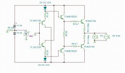
The important is that all wires go to a common point, at this current level the length of the cables is not that important , but it is not dificult to make them the same size.
Only need some wires connected like this , is not a big deal.
Attachments
![20121206_222957[1].jpg](/community/data/attachments/290/290776-1375131c75ef034aa561c91e828a61a5.jpg)
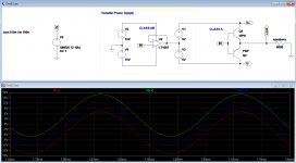
Here's something silly I came up with today. THD at full tilt of 7mA is something like 1 x 10^-5 give or take. The thing is, if the quiescent current in the output stage is 10 times or more than the silly -6.2mA of bias, then the fact that the output stage is knocked off balance doesn't matter that much for THD. Obviously, it performs even better with no DC offset current.
Attachments
You could bootstrap the collectors of the input transistors to the emitters of T3, T4.
I realize that is a normal technique, but my simulations show that it does not reduce distortion or anything good at all. I don't see the point of doing it. That's why I tie them to the rails instead. I do what makes sense to me.
- Status
- This old topic is closed. If you want to reopen this topic, contact a moderator using the "Report Post" button.
- Home
- Source & Line
- Digital Source
- dac I/V convertion with very low distortion