PCB is for stereo channel single ended?
If you do a PCB for ESS9018 will it be balanced?
also, what is the approx power draw for this circuit (as it is right now)?
If I made a version for the 9018 it will be very similar with this, but with another input , and more power hungry. The ess9018 have very low output impedance when use with parallel output , and this makes very difficult to design a good I/V converter without the use of feedback. But first I will finish this project.
This circuits use 30ma for the I/V part 6.2ma for the offset current source , that have 2 jumpers to inhibit if not needed. And the power drawn by the opamp of DC servo , 4ma if use opa2134 as I will use . the voltage is plus minus 15 volts.
If I made a version for the 9018 it will be very similar with this, but with another input , and more power hungry.
I would be more than happy to try one. Keep up the good work
")
Monday i made some home made board for testing, to be sure that every thing is ok before i send gerber files for production. I have already drill them but i stil need to buy components. Last week was a bit complicated and things advanced more slowly than i wish , but thats live.
Attachments
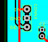
![board_12[1].jpg](/community/data/attachments/288/288354-83441163728f84028c7596f94f0465f7.jpg)
There are a bunch of people with 9018 DACs that would LOVE to try a version of this I/V
last week i visited a audio show with a lot of high end products, and that make me want to build an amplifier without feedback, and i am already testing some ideas to attain that. so a I/V converter design exclusively for ess9018 is not a priority right now.
But i have modified the pcb like i said in prior post, to use this I/V with the ess9018, but each pcb can only be connected to 2 dacs from ess9018 maximum, the ideal is one I/V pcb for each of the 8 dacs.
The output of the I/V converter boards will be paralleled, and only one servo and one buffer per channel will be needed the others 3 or 7 tagus pcb will run in slave and dont need the servo or the output buffer. I will post the connection schema for this.
In resume: is possible to use this pcb for the ess9018 , but we need at least 4 pcb per channel running in parallel. The ideal is 8 pcb per channel.
Last edited:
Big project, good luck and i look forward for your amp design.
I do not think that using feedback in the voltage amplifying stage is a problem but to make the output separate from the input feedback is certainly a good idea. I still have good memory when i first heard the Threshold Stasis, no sharpness and grain at all and a HUGE soundstage.
I do not think that using feedback in the voltage amplifying stage is a problem but to make the output separate from the input feedback is certainly a good idea. I still have good memory when i first heard the Threshold Stasis, no sharpness and grain at all and a HUGE soundstage.
Some people have sent me PM asking if i will sell it, or organise a group Buy, i have never do that before, but i think if a certain number of people are interested , it is possible to sell it for 12,5 euros each board and 10 euros if more than 8 pcb are required.
I have made a new email adress for this. So if you want to have this PCB sent me a email with your email address, DAC chip that you want to use and number of boards that you require. this is just for me to know the quantity of boards that i need to order. You dont need to pay nothing just yet.
note that it may take a month until the pcb are ready to send. I only do this at my spare time , when i have spare time, as my regular job takes me much time.
Attachments

Did you visit Zen Audio room ?last week i visited a audio show with a lot of high end products, and that make me want to build an amplifier without feedback, .
Big project, good luck and i look forward for your amp design.
I do not think that using feedback in the voltage amplifying stage is a problem but to make the output separate from the input feedback is certainly a good idea. I still have good memory when i first heard the Threshold Stasis, no sharpness and grain at all and a HUGE soundstage.
I have been away from audio from some years, and it seems that HD audio at 24bits is getting mature now. I have listening to some records at 24b/96K and i think it is a big step from cd 16bit quality. So i have to build an amplifier to get the best out of the increase resolution. I have some ecological concerns about pure class a amplifiers, i am thinking about using this very good idea from Matsushita
http://www.gtkc.net/files/class-a+.PDF
This was invented in the 70´s , nowadays we have much better components and i think it can be made a good amplifier based on this, i have already found some mosfet for the output. The output mosfets will have a current bias of 10 ampers and 1,8 volts each.
I also think that having feedback in the voltage stage is not a problem, but i will make the output current amplifier separate from the voltage amplifier , it will be like a giant buffer
. So i can experiment with different designs in the voltage amplifier.Here is the review with some measurements :http://www.avrevolution.com.au/SiteMedia/w3svc1114/Uploads/Documents/Quad_QSP_HFN.PDF
Interesting concept, a kind of current dumper. I have a recent QUAD amp that works quite well. The only thing i do not like is that it has quite drastic bandwidth limiting over 20kHz.
I tried to open the case to do some modification but so far i could not get inside.
No Joachim is not current dumper .
Is a amplifier in class A that has a floating power supply , and a amplifier in class AB that the only function is keep the midle of the power supply of class A amplifier equal to input signal, Both amplifiers have unitary voltage gain.
maybe this picture is more clear.
Attachments
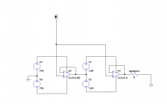
this type of circuit permits that the output stage works on class a but with low dissipation as the voltage across the output mosfet or transistors are very low. Ofcourse one has to be carefull with the class ab stage also, i have made some simulations and it seems to work very good.
- Status
- This old topic is closed. If you want to reopen this topic, contact a moderator using the "Report Post" button.
- Home
- Source & Line
- Digital Source
- dac I/V convertion with very low distortion