. R13/C2 looks potentially problematic and may make it prone to oscillation with inductive source impedance. This can usually be fixed with an input shorting cap, but point is to be aware of the issue so that you know what is going wrong and why in case of problems.
The bootstrapped cascodes creates a loop that is prone to oscillate at rf , R13/c2 is for adding loss at high frequencies, normally I have good results with this, in theory the c2 should be connected to positive rail, but in that way the PSRR at high frequency get worse.
I have see a lot of bootstapped cascode designs without any means to stop this oscillations to occur . But that is not much advised.
I ordered a bunch of ferrite beads a while back which have been sitting in a bin. These can be quite helpful. I wish I had tried them out sooner. They're easy to test on a prototype and instantly reusable. Like any reactive component, you have to know how to use them, but they can make you work less for the same result
Ferrite beads are non linear inductors ( hysteresis curve of ferrite ), some discourage the use of ferrite beads in audio circuits ,what is your experience with them , do they increase distortion?
Speaking of parasitic inductances and Just for curiosity , the most problematic situation that i enconter was with eGaN FETs , this type of FETs dont even have leads and have several souces and drain connections in parallel to lower to the extreme the parasitic inductance, at the speed they can switch the slightest inductance can cause ringing with enought voltage to damage them , especially in the gate that have maximum gate source voltage of 6 volts.
simulation with pcb traces parasitic inductances , in power switching is a must.
this is the link for the fets that i was talking (they are the future):
EPC2001
simulation with pcb traces parasitic inductances , in power switching is a must.
this is the link for the fets that i was talking (they are the future):
EPC2001
Last edited:
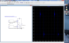
just for show how even a 0.5nH (a to220 lead has 12 nH of inductance) can have impact, i post this circuit the first without the drain parasitic inductance (500pH) the second with the added parasitic inductances, this is a extreme example and i just post it here for curiosity, in non swithing audio aplications this is not that bad .
with 2nH of parasitic the switch node reach 75 volts because of riging.
simulating this circuit without the pcb trace parasitic inductances can have drastic consequencies.
with 2nH of parasitic the switch node reach 75 volts because of riging.
simulating this circuit without the pcb trace parasitic inductances can have drastic consequencies.
Attachments
Last edited:
I'll use my current prototype as an example. I have an error correction buffer going to a simple IRF250 power buffer. The buffer is an advanced circuit of mine, the power buffer is just a source-follower biased at 500mA with a 10R resistor (driving 8" FR's). Without using ferrite beads, I might dicker around endlessly with the circuit, trying different compensations, RC snubbers, even regressing the design just to stop parasitic oscillations and reactivity that result in sibilance and fatigue. Maybe because I am using a 10R gate stopper for the IRF250, since I don't like the sound of a large gate stopper. But if I use ferrite beads, I can simply add one or two in series with the output of the line buffer, and this is pretty effective for eliminating sibilance in this application without losing the image depth and clarity that is so hard to achieve. Maybe not quite the same circuit, but it's worth a try.

I know this is a bit late, but what is the benefit of this? All the noise from the psu will be injected in the signal, not?
So why is it so clever?
For some reason I cannot quote a pic, I'm referring to this post:
http://www.diyaudio.com/forums/digi...rtion-very-low-distortion-26.html#post3133418
The supply could be a battery now that I think about it....
But, still, how on earth does the opamp work?!
That is a circuit that uses floating power supplies , first I think you should check this thread to grasp the concept, then if you still need I will explain the rest. Dont forget that the current that is injected to the circuit by the I1 will have to return to ground and the only path is by the output resistor.
http://www.diyaudio.com/forums/digi...-sen-evolution-minimalistic-iv-converter.html
My apologies coming in so late, and your question may already have been answered. But in case not:how do you come to 1k, i think is very low for a current source, if someone knows the real value please post.
So-called current-output DACs usually have a code-dependent and often rather low output resistance. They are NOT usually what we would call current sources. A better way to describe them is as having an output which must be connected to a low (even specified sometimes!) impedance input for accurate operation. Of course the standard approach is a voltage-feedback op amp connected as a transimpedance amp. Doing things with bipolars or JFETs as common-base or common-gate inputs is advantageous for a variety of reasons, but without global feedback you have to work pretty hard to have the distortion at the input itself be small and code-independent.
Short of enclosing a common-base or common-gate input design in a global feedback loop, one can also wrap a gain stage around the input devices to reduce the input resistance and equivalent inductance. Such a configuration is adroit at managing the fast rise-fall-time signals out of various DACs.
That is a circuit that uses floating power supplies , first I think you should check this thread to grasp the concept, then if you still need I will explain the rest. Dont forget that the current that is injected to the circuit by the I1 will have to return to ground and the only path is by the output resistor.
http://www.diyaudio.com/forums/digi...-sen-evolution-minimalistic-iv-converter.html
Sergio,
You are obviously a talent ...give us your vision otf the practical aplication.
I know you are still in Academia but this is about the music ....i want to hear your ideas....implemented.
One closer approximation in simulation and reality is to have some finite source impedance. This is particularly critical when various bootstrapping schemes are deployed.thanks jcx .That is also my experience. I will talk more about this later, as I think is very important.
Often to stabilize and compensate, about all that is required is some lumped C to common for the input. For really high frequencies you may want a little inductance to push resonances lower. I found about 300nH enough for a group of three paralleled 2SK170 parts (although that was not a bootstrapped drain design---probably of no consequence).
My apologies coming in so late, and your question may already have been answered. But in case not:
So-called current-output DACs usually have a code-dependent and often rather low output resistance. They are NOT usually what we would call current sources. A better way to describe them is as having an output which must be connected to a low (even specified sometimes!) impedance input for accurate operation. Of course the standard approach is a voltage-feedback op amp connected as a transimpedance amp. Doing things with bipolars or JFETs as common-base or common-gate inputs is advantageous for a variety of reasons, but without global feedback you have to work pretty hard to have the distortion at the input itself be small and code-independent.
Short of enclosing a common-base or common-gate input design in a global feedback loop, one can also wrap a gain stage around the input devices to reduce the input resistance and equivalent inductance. Such a configuration is adroit at managing the fast rise-fall-time signals out of various DACs.
That is a very old question
I have answer it myself here in post #8 :
http://www.diyaudio.com/forums/digital-source/221743-testing-pcm1794.html
The PCM1794 have a very high output impedance and is very easy to design a very low distortion I/V converter without feedback.
Sergio,
You are obviously a talent ...give us your vision otf the practical aplication.
I know you are still in Academia but this is about the music ....i want to hear your ideas....implemented.
Boas CeeVee,
Thanks,
Sorry, Can you Please specifies what you want, If you prefer send me a PM .
Thanks. Yes, that's the highest I've ever heard of and deserving of being thought of as a current source.That is a very old question
I have answer it myself here in post #8 :
http://www.diyaudio.com/forums/digital-source/221743-testing-pcm1794.html
The PCM1794 have a very high output impedance and is very easy to design a very low distortion I/V converter without feedback.
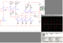
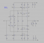
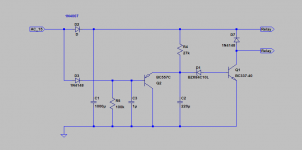
A forum member asked me to make a functional circuit for the pcm1794a, and this weekend I was in ltspice and did this, the idea was to have a more stable circuit. The resistance R3 can be a resistance of 180ohm in series with a potentiometer of 100 ohms, this will serve to cancel the DC offset at output, (R11,12,16,17) can have a lower value , with 10 Ohms value the input impedance is 7 ohms. Vcc is 15V and Vdd is -15V.
Attachments
- Status
- This old topic is closed. If you want to reopen this topic, contact a moderator using the "Report Post" button.
- Home
- Source & Line
- Digital Source
- dac I/V convertion with very low distortion