May i suggest other DAC.As Zinsula correctly remarked in #159, THD improves with rising Ibias/Idac relationship. But there´s a sweet-point of optimum bias depending on the chosen transistors. The PCM1795/1796 or 1798 DACs have lower currents (-3.5mA+-2mA) than the 1792/1794A and allow for lower power requirements. Sourcing of matched transistors may be easier if SMD casings can be used, due to lower currents and power requirements. You just need to increase the value of the Riv for same level output.
The probabely best match to the PCMs is the TI/BB SRC4392 asynchronous sample rate converter and DIX.
jauu
Calvin
AD1853 3mA pp 30pf
and it's brother
AD1955 8.6mA pp 100pf
i was told both are way better sounding than PCM1794.Especially AD1853.
I'm looking forward to build this I/V with something similar to this
USB DAC 2 - Hi-Resolution System
I like the AD1955 on paper, but the one thing that irks me somewhat is how the digital filters precision turns to crud when used with 192kHz. Now TI don't show their digital filters response for different sampling frequencies, so one only assumes that they are all the same, I wonder if this is a valid assumption. The trouble with the PCM1792/4 chips is that they are of old design and the engineers currently working at TI aren't totally familiar with how it works inside. At least that's the impression I got when talking to them.
Do you have to run the DAC diferential. Cant you just use the one output.... I mean for the summation after you need a circuit to Sum the outputs and make them unbalanced..with added circuit complexity. I know you gain some noise benefits and 2. harmonic cancellation, but at what cost...The balance could well be the simplicity of one circuit..
As dirkwright wrote, you can use a single phase of the differential outputs. There are both positive and negative consequences of doing this.
Some positive consequences: When used with a current-conveyer I/V (such as is the circuit under discsussion in this thread), or with a current feedback transimpedance I/V stage, reducing the magnitude of the signal current will usually reduce the distortion produced by the I/V stage. In addition, the amount of circuitry is reduced.
Some negative consequence: Slightly increased even order distortion and reduced SNR due to elimination of push-pull operation. In addition, the output impedance of a zero feedback I/V circuit, using a high impedance node for the output, will double versus the differential circuit. For example, with smms73's circuit, the I/V resistor effectively sets the output impedance. If both output phases were utilized, the I/V resistor could be reduced by half (and with it, the output impedance) and produce the same output voltage amplitude.
Last edited:
thanks Ken. what is the simulator that you use?
I use the freeware version of Spectrum Software's Micro-Cap.
Hi,
other current output DACs may be used alternatively. It seems to me that the actual DAC-cores of modern sigmadelta DACs are not the sonically decisive part but the periphery around that DAC-core. I found the mentioned ADIs sonically on par with the TIs, though an exact evaluation is very difficult, since small differences in clocks, PCB-layout, digital filter, etc. are of larger sonic influence than the DAC-core itself. The analog stages of the eval-boards of the ADI-DACs for example, equipped with OP275 OPAmps, simply sound terrible.
A interesting feature of the TIs and the AD1955 is the possibility to bypass the digital filter and to drive the DAC-core from a external digital filter at rates of up to 384kHz (see Anagram or PMD).
As to my knowledge the PCM1792/1794A feature a more powerful arithmetic machine for the digital filter than the (therefore cheaper) PCM1796 which may lead to small sonic differences.
jauu
Calvin
[...]BTW, your choice of 327 / 337 in most locations is a pretty good one for 2
reasons - who can guess what they are?
I like them because
- cheap ;-)
- low noise, low Rbb (thanks to Joachim who pointed that out some time ago)
- high beta (the ...-40 types), up to almost 100mA flat
- can carry quite high currents (although you of course are limited with a TO92 which has a thermal resistance junction - ambient of around 250K/W)
- up to 200-300 mA Ic almost flat Ic vs Uce curve (low early voltage)
")
dirk,
Correct, each ouput pin is never more than 3.9mA from the quiescent point. So, the pk-pk current output from EACH PIN can never be more than 7.8mA. I think confusion may stem from the fact that, indeed, no single pin can output 15.6mA. However, the pk-pk differential net CHANGE in current between pins is equal to 15.6mA. These currents are anti-phase, so you won't ever measure an in-phase 15.6mA from the output pins. If you look at the 'X' chart on post #155, you can see that the current difference between IoutP and IoutN swings from 7.8mA peak at one polarity, through BPZ where the 'X' arms cross, to 7.8mA peak at the opposite polarity. That's a peak-peak difference of 15.6mA.
Think of that 15.6mA net change in terms of the voltage a differential I/V stage would produce. If the I/V resistor were 1k, then IoutP by itself can produce a signal voltage of 1k x 7.8mApp(+/- 3.9mA) = 7.8Vpp. However, the outputs are differential, so we have IoutN to account for. IoutN by itself can also produce a signal voltage of 1k x 7.8mApp = 7.8Vpp. If fed anti-phase inputs from IoutP and IoutN both, a differential I/V will then produce a signal voltage of 2 x 7.8Vpp = 15.6Vpp. Which means that 15.6Vpp / 1K = 15.6mApp current is conducted through the I/V resistor.
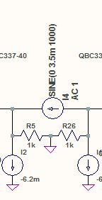
So, are you saying that we should use 15.6mA for the current generator in our simulations when it is connected in differential mode as shown for example in the attached figure?
Attachments
An issue with using DAC chips such as the AD1955 or AD1853 with a grounded-base I/V circuit is that the differential current output pins on these DACs want to see a common-mode input voltage that's offset above D.C. ground. For those ADI DACs, the figure is near +2.8VDC. The PCM179x series, on the other hand, wants to see a common-mode input voltage that's at D.C. ground. This issue can be addressed by level shifting the grounded-base input bias reference level from ground to the required D.C. offset, with a resistor biasing network and A.C. ground coupling capacitors.
Last edited:
So, are you saying that we should use 15.6mA for the current generator in our simulations when it is connected in differential mode as shown for example in the attached figure?
How the simulators handles differential signal source generator modeling might make giving an simple answer problematic. The most clear advice I can think of is to use whichever of the two current values for the source gen. which produces a 7.8mA peak and 15.6mA peak-peak signal current swing through the I/V resistor of the I/V stage being simulated - assuming, of course, that both output phase currents are being differentially utilized.
Last edited:
So, are you saying that we should use 15.6mA for the current generator in our simulations when it is connected in differential mode as shown for example in the attached figure?
One other point. When modeling a two-terminal differential signal source you should set the internal source impedance equal to twice that of a single DAC output pin impedance. For example, if the impedance of a signle DAC output pin were 1K, then set the modeled generator internal impedance to 2K. That is because the DAC differential outputs are effectively in series with each other with respect to a common, differentially driven load. Which means their individual output impedances are also in series, again with respect to a common, differentially driven load.
An increased source impedance has beneficial THD implications for the I/V stage. Although, the doubling of the signal current magnitude then degrades the I/V stage THD.
Last edited:
One other point. When modeling a two-terminal differential signal source you should set the internal source impedance equal to twice that of a single DAC output pin impedance. For example, if the impedance of a signle DAC output pin were 1K, then set the modeled generator internal impedance to 2K.
That is because the DAC differential outputs are effectively in series with each other with respect to a common, differentially driven load. Which means their individual output impedances are also in series, again with respect to a common, differentially driven load.
OK, thanks.
The outputs from the current generator in the image I posted above are 180 degrees out of phase and half the value of the generator, so it appears to be functioning as a differential current source. I've done this with the voltage generator in other circuits in Tina also with the same effect.
(edit: whoops, made a mistake. Setting the current generator to 7.8mA produces that amount on BOTH pins of the generator, not half like I thought)
Last edited:
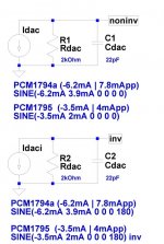
Hi,
in Mono mode the DACs currents just double to -12.4mA | +-7.8mApp for the PCM1794a, or -7mA | +-4mApp for the PCM1795.
Now the outputs of L+ and R- must be connected together as noninv current summing point. Same applies L- and R+ for the inv sum. The DAC must be set to mono mode and the appropriate channel Left or Right selected via setting of Pin1 and Pin2 of the Chip.
As mentioned before low THD requires that the signal current stroke remains small against the current conveying transistor´s bias current. As such a PCM1795 in Mono mode has similar current values and this results in similar IV-distortion figures as a PCM1794a in stereo mode. On the other hand will a PCM1794a in mono mode lead to increased THD of the IV-stage.
Higher DAC output currents are not neccessarily a improvement.
If for example one bypasses the digital filter section of the DAC chips a PCM1795 in Mono mode may be better than a PCM1794a in stereo mode.
jauu
Calvin
Last edited:
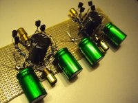
Good circuit
I have built quite a few circuits based on these principles using mirrors to
sum the +and- phases then that current modulating cascoded OP stage.
DAC's , front ends of open loop SS power amplifiers and even a mic pre that
have a bal IP and SE OP (fully complimentary).
I have also implemented the same type of OP stage with those cross
coupled darlingtons. They do work very well to linearise non linear base currents and capacitances.
It's really a design twist of the 'Baxandall pair' connected BJT's, using the
'error' current from the bases of the main OP BJT's as + feedback. Your sim
numbers tell the story.
It all works just like it should in real life too with one gotcha - stability.
You may or may not have stability issues. It depends on layout etc. C1 will
certainly help but you may need additional base stoppers in either the main
OP BJT's or the 'helpers'.
Once you get the whole thing on a board and prototyped, it really is worth
having a good listen with and without all the Baxandall collector connections
to up/down labelled points. With these connected, the distortion will
certainly measure a lot better, however it may not actually sound better.
IME, with all these small + feedback loops, the sound can be worse. Without
them it is often more natural, but you won't get the super low dist numbers.
I'll be interested if you have similar results with this design. Keep us posted.
BTW, your choice of 327 / 337 in most locations is a pretty good one for 2
reasons - who can guess what they are?
T
Nice to hear that someone has already test the concept, and it work.
I have thought of this idea a long time ago when i needed a high voltage amplifier for a valve circuit (the input was a valve), but it was never build and it remain forgotten until last week, when I remembered that could be a good idea for a i/v converter. I never heard of 'Baxandall pair' but i will investigate.
STABILITY:
stability is one of the biggest problems in audio circuits, and for me is a very important matter.
Is perhaps the number one reason as otherwise very good concepts sound bad,. And is also one of the reason people tend to prefer a simple circuit versus a more complex one, as normaly, in many schemas there is no attempt to use stability measures
I do not know which methods you use to stabilize the circuit but rely only in base stoppers and good pcb layout is important but not enough.
this topology is very fast, so there are many possibilities for instability to build up. the
solution is to slow it down.
Today i have spend some time analysing possible nodes where stability can be a problem, and i will post soon the results.
After the circuit is rock solid stabilized there will be no reasons to sound bad.
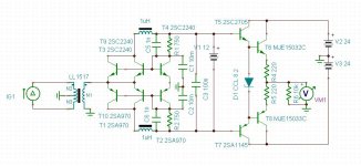
Hi,
the current mirror reminds of an ´full Wilson´. See for example sboa046 "IMPLEMENTATION AND APPLICATIONS OF CURRENT SOURCES AND CURRENT RECEIVERS" of TI/BB.
A ´complementary full Wilson´ is the Zetex part ZDS1009 in SM-8 casing, which might be a possible replacement part for the discrete BC327/337, because of the matching issues/oscillation issues of these cascoded current mirrors.
Well You can of course imbalance the whole stage by increasing the lower ccs bias current, but what´s the deal in designing a symmetrical stage just to spoil its symmetry right away to accommodate for the DAC? Yes, a dedicated CCS would mean more complexity and a slight noise penalty. But a simple JFET ccs is the simplest and the least noisy ccs You can have here, just two parts, a JFET and an R. Noise figures will be slightly higher (1-2dB), but still be well below -110dBV.
In the case of a current sourcing DAC with an offset current a SE-circuit, basically using just the upper half and a ccs towards the negative supply, would be more elegant and less complex.
I agree with Terry, that the multiple loops and cascoded mirrors may give stability problems and may sonically not be as overwhelming as the distortion figures imply (which have yet to be proofed in reality).
In my tests a simple SE-grounded base stage (rem. "Jocko" or SEN) certainly sounded better than a similar, but more complex and lower THD Hawksford current steering I/V stage.
As Zinsula correctly remarked in #159, THD improves with rising Ibias/Idac relationship. But there´s a sweet-point of optimum bias depending on the chosen transistors. The PCM1795/1796 or 1798 DACs have lower currents (-3.5mA+-2mA) than the 1792/1794A and allow for lower power requirements. Sourcing of matched transistors may be easier if SMD casings can be used, due to lower currents and power requirements. You just need to increase the value of the Riv for same level output.
The probabely best match to the PCMs is the TI/BB SRC4392 asynchronous sample rate converter and DIX.
You may linearize input impedance with the Zobel, but You put a burden on the DAC that needs to charge/discharge the Cap. It slows and rounds the current steps of the DAC (lower bandwidth) and is often used with OPamp-IVs featuring ´too slow´ OPamps. I typically found that such caps were no improvement sonically, but quite the opposite.
jauu
Calvin
Thanks for the tip about ZDS1009 and the interesting literature about current mirrors , i will see if i arrange time to read it.
In the last circuit i have post the distortion is smaler with the -6.2ma off ofset that without them.
about the stability, i have talk about that in my last post, and the final circuit will not have stability problems.
I have been posting the evolution of this project, i start to doubt if this is the best thing to do in this forum, but ok.
the idea of using a small current output dac as pcm1795/96 is a very good one, i will see the datasheet on this dac.
The input snuber will have very low interaction in the audio frequency, and is not a burden for the dac.
- Status
- This old topic is closed. If you want to reopen this topic, contact a moderator using the "Report Post" button.
- Home
- Source & Line
- Digital Source
- dac I/V convertion with very low distortion