Okay, today I took the time to enter the circuit in my simulator. I must say, I'm impressed. I randomly substituted all manner of various transistors throughout the circuit, and found the THD indeed remains in the vicinty of -140dB, although the specific profile of hamonics vary. This is highly unusal behavior for an open-loop bipolar circuit in my experience. Well done.
thanks Ken. what is the simulator that you use?
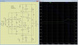
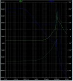
THD seems really low, but input impedance rises above 1MHz with some weird up-and downs, especially around 66MHz, where seemingly a resonance builds up.
I have been analysing this, and the conclusions is
the rising of the impedance is due to the lost of gain of the input transistors as the frequency goes up.
The dips and ups around 66Mhz are due to the interaction of the dac output capacitance (22pf) with the input.
The best soluction is to use a snubber (zobel) in the input.
In the pictures below is the output and input gain and phase with the snubber and without it.
Its very important to use the snubber in the circuit.
Attachments
The dynamic signal current swing from EACH output pin is 3.9mA peak single-ended. Therfore, the peak-peak signal current swing from EACH output pin is 7.8mA single-ended. The DIFFERENTIAL output signal net current change for a given channel then is 7.8mA peak, and 15.6mA peak-peak.
I'm sorry this does not make sense, particularly in light of the chart in post #155.
I'm sorry this does not make sense, particularly in light of the chart in post #155.
Let's walk this through. The table in that chart you refer to shows two anti-phase output signals, IoutN and IoutP. You can read the peak-peak current magnitude for either output phase directly from the table, which is 10.1mA minus 2.3mA = 7.8mA. The signal current swing is centered around a BPZ (Bipolar Zero) bias current of 6.2mA. So, 10.1mA minus 6.2mA = 3.9mA peak, from BPZ, and then 6.2mA minus 2.3mA = 3.9mA for the opposite peak, from BPZ - from either output pin. The resulting 7.8mA pk-pk signal current swing is abailable from BOTH IoutP and IoutN. Now, since the two output signal currents move in anti-phase (they are differential), the differential peak-peak net signal current change is 2 x 7.8mA = 15.6mA.
Last edited:
TAGUS
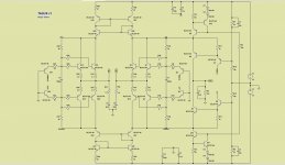
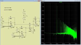
Is time to present to you guys, the almost finished differential version that i resolve to call TAGUS.
It has a new current mirror that is also a voltage mirror.
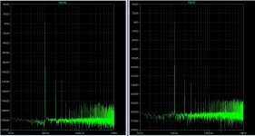
The distortion is measure with a 500ohm/22pf input
and is 0.000130% at 7.8ma p-p at each input.
and only 0.000055% at 3.9ma p-p.
Below are the schema and the fft for 7.8ma and 3.9ma
I will talk about it later because today going to be a busy day, hope you enjoy.
Is time to present to you guys, the almost finished differential version that i resolve to call TAGUS.
It has a new current mirror that is also a voltage mirror.
The distortion is measure with a 500ohm/22pf input
and is 0.000130% at 7.8ma p-p at each input.
and only 0.000055% at 3.9ma p-p.
Below are the schema and the fft for 7.8ma and 3.9ma
I will talk about it later because today going to be a busy day, hope you enjoy.
Attachments
I am thinking in building this:
Modular audio DAC
and change only the I/V convertor, i like the modular idea.
What you guys think, if you have or know were to find a better pcb for a dir9001 and pcm1794a please let me know. I really dont have the time to design my one, thanks in advance.
Modular audio DAC
and change only the I/V convertor, i like the modular idea.
What you guys think, if you have or know were to find a better pcb for a dir9001 and pcm1794a please let me know. I really dont have the time to design my one, thanks in advance.
Cool, i like that mirror.
have you ever seen one like this?
I am thinking in building this:
Modular audio DAC
and change only the I/V convertor, i like the modular idea.
What you guys think, if you have or know were to find a better pcb for a dir9001 and pcm1794a please let me know. I really dont have the time to design my one, thanks in advance.
Are you aware that DIR 9001 only does 96k ?
The CS 8416 module does 192k.
I'm thinking you want to do the PCM1794A justice, so 192k!?
...and be prepared for a huge hunt for the TORX thingies....very scarce .
CV
Last edited:
Do you have to run the DAC diferential. Cant you just use the one output.... I mean for the summation after you need a circuit to Sum the outputs and make them unbalanced..with added circuit complexity. I know you gain some noise benefits and 2. harmonic cancellation, but at what cost...The balance could well be the simplicity of one circuit..
Let's walk this through. The table in that chart you refer to shows two anti-phase output signals, IoutN and IoutP. You can read the peak-peak current magnitude for either output phase directly from the table, which is 10.1mA minus 2.3mA = 7.8mA. The signal current swing is centered around a BPZ (Bipolar Zero) bias current of 6.2mA. So, 10.1mA minus 6.2mA = 3.9mA peak, from BPZ, and then 6.2mA minus 2.3mA = 3.9mA for the opposite peak, from BPZ - from either output pin. The resulting 7.8mA pk-pk signal current swing is abailable from BOTH IoutP and IoutN. Now, since the two output signal currents move in anti-phase (they are differential), the differential peak-peak net signal current change is 2 x 7.8mA = 15.6mA.
This does not agree with 5th element's analysis.
Each Iout pin is never more than 3.9mA from the quiescent point. So, the differential p-p current output can never be more than 7.8mA. When one output is at -2.3mA the other is at -10.1mA. There is no room in that chart for 15.6mA.
so no, I don't understand your analysis. Can someone else please explain what he's talking about to me?
Do you have to run the DAC diferential. Cant you just use the one output.... I mean for the summation after you need a circuit to Sum the outputs and make them unbalanced..with added circuit complexity. I know you gain some noise benefits and 2. harmonic cancellation, but at what cost...The balance could well be the simplicity of one circuit..
You can take the output from one Iout pin only, but the distortion will be much higher. DAC designers are in a tough fist fight over spec's and they realized that if they provided balanced outputs with an attached circuit that had a high CMRR, they could reduce distortion even further and thus sell more DAC chips.
Are you aware that DIR 9001 only does 96k ?
The CS 8416 module does 192k.
I'm thinking you want to do the PCM1794A justice, so 192k!?
...and be prepared for a huge hunt for the TORX thingies....very scarce .
CV
i realy don't have any exprience in dacs. this is my first. i just already have the dir9001. but im open to sujestions. do you know any good pcb for the chip you sujest?
Do you have to run the DAC diferential. Cant you just use the one output.... I mean for the summation after you need a circuit to Sum the outputs and make them unbalanced..with added circuit complexity. I know you gain some noise benefits and 2. harmonic cancellation, but at what cost...The balance could well be the simplicity of one circuit..
in my case i only use two of the non differential tagus circuits and use balanced connection , and let the power amplifier do the differentiation. but i like the chalange of making it diferential at the beginning.
Is time to present to you guys, the almost finished differential version that i resolve to call TAGUS.
It has a new current mirror that is also a voltage mirror.
The distortion is measure with a 500ohm/22pf input
and is 0.000130% at 7.8ma p-p at each input.
and only 0.000055% at 3.9ma p-p.
Below are the schema and the fft for 7.8ma and 3.9ma
I will talk about it later because today going to be a busy day, hope you enjoy.
Here are the I/V of the texas datasheet and the FFT just for comparing.
have you ever seen one like this?
Good circuit
I have built quite a few circuits based on these principles using mirrors to
sum the +and- phases then that current modulating cascoded OP stage.
DAC's , front ends of open loop SS power amplifiers and even a mic pre that
have a bal IP and SE OP (fully complimentary).
I have also implemented the same type of OP stage with those cross
coupled darlingtons. They do work very well to linearise non linear base currents and capacitances.
It's really a design twist of the 'Baxandall pair' connected BJT's, using the
'error' current from the bases of the main OP BJT's as + feedback. Your sim
numbers tell the story.
It all works just like it should in real life too with one gotcha - stability.
You may or may not have stability issues. It depends on layout etc. C1 will
certainly help but you may need additional base stoppers in either the main
OP BJT's or the 'helpers'.
Once you get the whole thing on a board and prototyped, it really is worth
having a good listen with and without all the Baxandall collector connections
to up/down labelled points. With these connected, the distortion will
certainly measure a lot better, however it may not actually sound better.
IME, with all these small + feedback loops, the sound can be worse. Without
them it is often more natural, but you won't get the super low dist numbers.
I'll be interested if you have similar results with this design. Keep us posted.
BTW, your choice of 327 / 337 in most locations is a pretty good one for 2
reasons - who can guess what they are?
T
i realy don't have any exprience in dacs. this is my first. i just already have the dir9001. but im open to sujestions. do you know any good pcb for the chip you sujest?
Yep !
Same site you referenced but since you have the DIR 9001 already make it , PCB is in the site and it's a modular concept you are after, so you can easily upgrade this module anytime.
Hi,
the current mirror reminds of an ´full Wilson´. See for example sboa046 "IMPLEMENTATION AND APPLICATIONS OF CURRENT SOURCES AND CURRENT RECEIVERS" of TI/BB.
A ´complementary full Wilson´ is the Zetex part ZDS1009 in SM-8 casing, which might be a possible replacement part for the discrete BC327/337, because of the matching issues/oscillation issues of these cascoded current mirrors.
Well You can of course imbalance the whole stage by increasing the lower ccs bias current, but what´s the deal in designing a symmetrical stage just to spoil its symmetry right away to accommodate for the DAC? Yes, a dedicated CCS would mean more complexity and a slight noise penalty. But a simple JFET ccs is the simplest and the least noisy ccs You can have here, just two parts, a JFET and an R. Noise figures will be slightly higher (1-2dB), but still be well below -110dBV.
In the case of a current sourcing DAC with an offset current a SE-circuit, basically using just the upper half and a ccs towards the negative supply, would be more elegant and less complex.
I agree with Terry, that the multiple loops and cascoded mirrors may give stability problems and may sonically not be as overwhelming as the distortion figures imply (which have yet to be proofed in reality).
In my tests a simple SE-grounded base stage (rem. "Jocko" or SEN) certainly sounded better than a similar, but more complex and lower THD Hawksford current steering I/V stage.
As Zinsula correctly remarked in #159, THD improves with rising Ibias/Idac relationship. But there´s a sweet-point of optimum bias depending on the chosen transistors. The PCM1795/1796 or 1798 DACs have lower currents (-3.5mA+-2mA) than the 1792/1794A and allow for lower power requirements. Sourcing of matched transistors may be easier if SMD casings can be used, due to lower currents and power requirements. You just need to increase the value of the Riv for same level output.
The probabely best match to the PCMs is the TI/BB SRC4392 asynchronous sample rate converter and DIX.
You may linearize input impedance with the Zobel, but You put a burden on the DAC that needs to charge/discharge the Cap. It slows and rounds the current steps of the DAC (lower bandwidth) and is often used with OPamp-IVs featuring ´too slow´ OPamps. I typically found that such caps were no improvement sonically, but quite the opposite.
jauu
Calvin
This does not agree with 5th element's analysis.
Each Iout pin is never more than 3.9mA from the quiescent point. So, the differential p-p current output can never be more than 7.8mA. When one output is at -2.3mA the other is at -10.1mA. There is no room in that chart for 15.6mA.
so no, I don't understand your analysis. Can someone else please explain what he's talking about to me?
dirk,
Correct, each ouput pin is never more than 3.9mA from the quiescent point. So, the pk-pk current output from EACH PIN can never be more than 7.8mA. I think confusion may stem from the fact that, indeed, no single pin can output 15.6mA. However, the pk-pk differential net CHANGE in current between pins is equal to 15.6mA. These currents are anti-phase, so you won't ever measure an in-phase 15.6mA from the output pins. If you look at the 'X' chart on post #155, you can see that the current difference between IoutP and IoutN swings from 7.8mA peak at one polarity, through BPZ where the 'X' arms cross, to 7.8mA peak at the opposite polarity. That's a peak-peak difference of 15.6mA.
Think of that 15.6mA net change in terms of the voltage a differential I/V stage would produce. If the I/V resistor were 1k, then IoutP by itself can produce a signal voltage of 1k x 7.8mApp(+/- 3.9mA) = 7.8Vpp. However, the outputs are differential, so we have IoutN to account for. IoutN by itself can also produce a signal voltage of 1k x 7.8mApp = 7.8Vpp. If fed anti-phase inputs from IoutP and IoutN both, a differential I/V will then produce a signal voltage of 2 x 7.8Vpp = 15.6Vpp. Which means that 15.6Vpp / 1K = 15.6mApp current is conducted through the I/V resistor.
Last edited:
- Status
- This old topic is closed. If you want to reopen this topic, contact a moderator using the "Report Post" button.
- Home
- Source & Line
- Digital Source
- dac I/V convertion with very low distortion