As the doubt about the need of matched transistors appears very often, i post here the same circuit with bc327 for pnp and bc547c for all npn, they are very different and the thd is 0.000008% (7,8ma/100k), its no need for matched transistors. hope this end the subject, and we can move on.
Okay, today I took the time to enter the circuit in my simulator. I must say, I'm impressed. I randomly substituted all manner of various transistors throughout the circuit, and found the THD indeed remains in the vicinty of -140dB, although the specific profile of hamonics vary. This is highly unusal behavior for an open-loop bipolar circuit in my experience. Well done.
A circuit idea like this appears every 10 years maximum and that in a surrounding where many search the holy grail in I/V converters. Now that i see it it is so obvious as it would have being there all the time. Certainly a stroke of genius in my book. Lets see what it brings in a practical implementation.
Ideally, voltage gain would be much higher, increasing as the virtual ground impedance of the grounded-base stage input is reduced. But what matters here is current flow. The circuit conveys DAC output current to the 400R I/V resistor, while isolating the DAC output from the voltage swing developed across the I/V resistor.
OK, then I don't understand this circuit.
I'm refering to voltage gain as seen from between the grounded-base emitters and the I/V resistor. Let's take a couple examples for illustration. If the output voltage across the 400R I/V resistor were 1VRMS, it would mean the peak current from the DAC were 3.5mA. Now, if the input impedance of the grounded-base emitters were 2R, then the peak input voltage devloped at those emitters (and at the DAC's current output pin) will be: 2R x 3.5mA = 7mV peak = 4.9mVRMS. The overall voltage gain would then be: 1V / 4.9mV = x204 = 46dB.
If the grounded-base input impedance were 1R, then the voltage gain would be x408, or about 52dB. The lower the input impedance, the greater the apparent voltage gain. Ideally, there would be zero apparent input voltage, as the input is supposed to be an A.C. ground with an impedance of zero Ohms. This could give the appearance of infinite voltage gain (divide by zero error aside), but this would be an illusion, as the circuit is conveying current not amplifying voltage.
The apparent input to output voltage gain is not really of concern here. The conveyance of current by the circuit is what matters. DAC signal current is input to an (ideally) zero impedance virtual ground and conveyed through an I/V resistor, which in turn produces the signal voltage according to Ohm's law.
Last edited:
The most simple solution for that is an Opamp setup for series feedback. Going into Pin 2 and grounding Pin 3. The "real" part of even a low input impedance current feedback Opamp like the LME49713 is around 50 Ohm though. The "Zero" Ohm input impedance is a result of the feedback. The topology presented here could also being setup for series feedback but then we loose the open loop character. It is the old discussion about what sounds best and what measures best.
Regal,
What is the source of that 670R figure? I'm not disputing it, it's just that the output impedance of the PCM179X series has been shrouded in mystery because T.I. hasn't seen fit to document it in their datasheets. By the way, the number I've seen reported (unofficially and indirectly) is 100k, supposedly from T.I. engineers in Germany.
The same way one measures the input impedance of an I/V stage just in reverse, we know the ipk-pk output of the PCM179x, feed it an I2S signal encoded with a sine wave from LSB to MSB, DAC output to and I/V of known input resistance (10 ohm resistor to ground), scope on top of resistor. Ohm's law from there.
The "unofficial" 100k number comes from just measuring the 4 bits that are supposedly R2R (Ti calls them current segment on their functional block diagram) but the base of the architecture is the "advanced segment modulator."
Hi,
I don´t know why, but TI is very secretive about the output impedance of their audio DACs. I got told figures of 2M||22pF for the PCM1792/1794a, but I regard those numbers as simply wrong. I use 2k||22pF instead.
Unfortunately the output impedance varies widely with different DACs.
The older Colinear 20Bit PCM63 is specced at 670Ohms. The 24Bit PCM1704 is specced at 1kOhm. Non-Audio current output DACs like the DAC5675, DAC902, etc are specced at 200k-300k, 5pF-12pF. So I assume that the PCM179x-series has similar to the other audio-DACs rather lowish impedance values.
In simulation, I use current sources with parallel R and C. The offset current beeing as stated in the datasheet for current sourcing DACs-6.2mA or -3.5mA and the amplitude 3.9mA, resp. 2mA.
Of course this IV-stage needs a dedicated current sink towards the negative supply to null the DACs centre current, for example a simple source resistor degenerated JFET.
Did a sim of the IV-stage also, using the BC807/BC817 Philips/NXP models (SMD equivalent to BC327/337). THD seems really low, but input impedance rises above 1MHz with some weird up-and downs, especially around 66MHz, where seemingly a resonance builds up. Everything else sims well. There´s a input offset of a couple of tens of mVs which may be cancelled with a simple Poti betwee the supply lines, the wiper feeding into the bases of Q2/Q3. There´s also an output offset of a couple of hundreds of mVs, which may not be serious, if a following buffer stage is AC-coupled. Else it must be taken care of.
jauu
Calvin
Last edited:
In simulation, I use current sources with parallel R and C. The offset current beeing as stated in the datasheet for current sourcing DACs-6.2mA or -3.5mA and the amplitude 3.9mA, resp. 2mA.
Of course this IV-stage needs a dedicated current sink towards the negative supply to null the DACs centre current, for example a simple source resistor degenerated JFET.
Did a sim of the IV-stage also, using the BC807/BC817 Philips/NXP models (SMD equivalent to BC327/337). THD seems really low, but input impedance rises above 1MHz with some weird up-and downs, especially around 66MHz, where seemingly a resonance builds up. Everything else sims well. There´s a input offset of a couple of tens of mVs which may be cancelled with a simple Poti betwee the supply lines, the wiper feeding into the bases of Q2/Q3. There´s also an output offset of a couple of hundreds of mVs, which may not be serious, if a following buffer stage is AC-coupled. Else it must be taken care of.
jauu
Calvin
Hi calvin,
For compensate the output offset current of the dac, it only needs to increase the upper current source, this also serves to trim the output voltage offset.
thanks to bring to my attention the problem of input impedance, add c4 and c5 should resolve the problem.
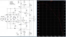
The output capacitor C1 is now 4n4 for filtering hi freq noises from dac, below is the circuit with some alterations. And the frequency response, as you see there is no instability now.
Only today i realize that pcm1794 has 7.8ma peak to peak, i was thinking it was 7.8ma peak, so all prior result of harmonic distortion have been made at 15,6ma peak to peak, at 7,8ma p-p the distortion is smaler, this version i apresent today has:
0.000006% at 10kohm input
0.000024% at 1Kohm input
0.000043% at 500ohm input
0.000096% at 200ohm input
Attachments
Only today i realize that pcm1794 has 7.8ma peak to peak, i was thinking it was 7.8ma peak, so all prior result of harmonic distortion have been made at 15,6ma peak to peak, at 7,8ma p-p the distortion is smaler, this version i apresent today has:
I am sure this has perhaps been mentioned but the above isn't quite true either. The PCM1794s outputs sit at a current of -6.2mA when the analogue outputs are doing nothing. That +-7.8mA then swings about this point from -14mA up to 1.6mA. The final summing stage in the TI implementation handles this and cancels the common offset from the differential outputs.
I am sure this has perhaps been mentioned but the above isn't quite true either. The PCM1794s outputs sit at a current of -6.2mA when the analogue outputs are doing nothing. That +-7.8mA then swings about this point from -14mA up to 1.6mA. The final summing stage in the TI implementation handles this and cancels the common offset from the differential outputs.
So, it is actually max 15.6mA p-p across the two Iout pins? If I were to simulate this with a differential current source, I should set it to 15.6mA p-p? I find this confusing.
Hmm that's the way I've always assumed it worked, but thinking about it. The output with 2VRMS uses 750R feedback resistors in the I/V converter, these then feed into the differential/summing configured opamp which has a 560/270 divider before it.
2V RMS = 5.64 volts peak to peak.
For this to be on the output of the differential opamp it would need to receive 5.64/2 volts peak to peak on each input pin, so 2.82 volts peak to peak. But in this case there is a potential divider before hand which halves the signal at each pin, so you'd need to multiple 2.82 by 2 again, to get the voltage back up. This leaves you at each I/V stage needing to output 5.64 Vp-p for the total output to = 2VRMS.
5.64/750 = 7.52, which is close enough to 7.8mA. So it would seem my assumption was incorrect and I've talked to people at TI using +-7.8mA and no one has ever corrected me! It is indeed swinging +-7.8/2. This keeps the entire current at the outputs negative for the entire output swing, which probably makes some sort of sense as to how the DAC works, otherwise, why offset the output at all?
The PCM1794A current outputs can be confusing. There are four output pins, +L, -L, +R, -R. Each output pin sinks a quiescent bias current of -6.2mA to ground. To help clarify the polarity of this bias current, an passive resistor I/V, for example, would develop a positive bias voltage with respect to ground from this bias current.
The dynamic signal current swing from EACH output pin is 3.9mA peak single-ended. Therfore, the peak-peak signal current swing from EACH output pin is 7.8mA single-ended. The DIFFERENTIAL output signal net current change for a given channel then is 7.8mA peak, and 15.6mA peak-peak.
The dynamic signal current swing from EACH output pin is 3.9mA peak single-ended. Therfore, the peak-peak signal current swing from EACH output pin is 7.8mA single-ended. The DIFFERENTIAL output signal net current change for a given channel then is 7.8mA peak, and 15.6mA peak-peak.
Last edited:
Hi,
You can't compensate the DAC centre current by increasing the upper ccs current. The DACs current is taken by the lower ccs (it's a current sourcing DAC). This would imbalance the symmetry of the stage since the lower half of the input stage of the circuit runs at higher current levels. Also heat dissation might become a problem, especially if the PNPs were SMDs. Therefore I only suggest a dedicated current sink from the DAC output to the negative supply.
Compensating for the Input Offset Voltage at the bases of Q2/3 changes the Output offset voltage considerably as well. Vice versa changes the compensation of Output Offset the Input Offset slightly. Getting both compensated might become a bit delicate. Since One probabely wants to add a Buffer Stage anyway it might be best to compensate only for the Input Offset and AC couple to the Buffer.
jauu
Calvin
In this case, i cannot agree with you.You can't compensate the DAC centre current by increasing the upper ccs current. [...]
I think it's perfectly possible to unbalance the two current sources by 6.2 mA. One ccs has to deliver 6.2mA more than the other one sinks, if the DAC will sink this amount. It's even more elegant than a separate ccs.
Important is that the emitter current of Q3 and Q6 (Post #150) is equal (as will the currents in the input transistors be).
Regarding dissipation, you should always run much higher currents in such I/V's than the current swing of the DAC is, in order to keep input resistance low and stable (impedance of emitter follower depends from current and base impedance*beta).
If you run into dissipation problems because of an imbalance of 6.2mA, you are already biasing way to low.
Hi,
You can't compensate the DAC centre current by increasing the upper ccs current. The DACs current is taken by the lower ccs (it's a current sourcing DAC). This would imbalance the symmetry of the stage since the lower half of the input stage of the circuit runs at higher current levels. Also heat dissation might become a problem, especially if the PNPs were SMDs. Therefore I only suggest a dedicated current sink from the DAC output to the negative supply.
Compensating for the Input Offset Voltage at the bases of Q2/3 changes the Output offset voltage considerably as well. Vice versa changes the compensation of Output Offset the Input Offset slightly. Getting both compensated might become a bit delicate. Since One probabely wants to add a Buffer Stage anyway it might be best to compensate only for the Input Offset and AC couple to the Buffer.
jauu
Calvin
Yes, sorry my mistake. you have to increase the lower current source to null the output offset created by the current imbalance of dac.
There is no problem in imbalance the symetry of the input stage, as this only increase the 2º harmonic distortion, and as this distortion are in phase they will be cancelled by the diferential stage.
Adding another current source in the input as you suggest will increase complexity and noise .
In respect to dissipation i must agree with zinsula, and you can always use more input bjt in parallel, to decrease individual bjt dissipation.
- Status
- This old topic is closed. If you want to reopen this topic, contact a moderator using the "Report Post" button.
- Home
- Source & Line
- Digital Source
- dac I/V convertion with very low distortion