Current conveyors are circuits which have a low-impedance input and a high-impedance output. They may be as simple as a biased common-gate or common-base transistor (see EUVL’s “ Zen -> Sen -> Cen, evolution of a minimalistic IV Converter” thread for example). Such current conveyors are noninverting, that is, the signal polarities of input and output are the same. Here is an example of a current conveyor that inverts signal polarity, which adds versatility when used with so-called current-output DACs. For example, if one wishes to convert from differential DAC outputs to a single-ended voltage, rather than the traditional I-V converters using opamps, with resistive feedback feeding a differential amp (usually using four resistors and another opamp), the output of a noninverting current conveyor can simply be strapped to the output of this inverting one. Alternatively, two of these can be used and the output of one (sans termination resistor) can be fed directly to the input of the other, and the final single-ended circuit output taken from the two-input one. Aside from the small excess delay of one signal path the conversion will be accurate.
With moderately-high-current output DACs the resulting signal may be large enough, and the terminating resistor sufficiently small in value, as to be suitable for driving short lengths of cable to the preamp. Alternatively, a voltage buffer of sufficiently high performance can be provided.
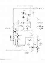
The schematic attached is an example of the topology, which can be optimized for a wide range of specific DACs. In this case the design supports a bipolar input of +/- 8mA, with symmetrical clipping occurring at +/- 9mA. With the resistor values shown the voltage swing is +/- 8V operating, +/-9V overload. One might well ask why such high voltage rails are needed when the output swings are relatively modest, and the answer is in order to support significant voltage drops associated with FETs and various ballasting and biasing resistors, in turn for lower noise and distortion.
There are several features worthy of note:
The input is a Boxall base-current-corrected complementary pair. The variations of Q1 base current with signal level and temperature are mostly removed by Q2, which returns them to the Q1 emitter. Q2 is biased by a current generator consisting of Q7, Q15, and R11, adjusted for a constant current of about 1mA. The precise value of the current is not too important because it becomes part of the output current of that stage, so what is removed from the input current is restored at the output, except for the base current of Q2. A lower bias current can be used although 1mA is about optimal for bandwidth and transient response. Q1 and Q2 can be selected from your favorite high-beta moderate-frequency bipolars. Q2 could be a much faster part, since it operates at a Vce of the Vbe of Q1. However, such parts are often lower beta, and the noise in Q2 base current could become significant. Addis has also noted problems with oscillation, although a small resistor in series with the Q1 emitter can control these.
The output of the Boxall common-base input stage passes to a current mirror constructed of JFETs and DMOS FETs. Note that the topology just emulates a simple predistorting bipolar current mirror, using cascoded FETs. The recommended devices are matched BF862 and (ideally) matched 2N7000 (the matching of the DMOS is much less critical). The 2N7000 parts run a little warm and may benefit from some heatsinking.
Biasing of the FETs, required to have the FETs in a useful operating region, is via floating voltage generators. The precise voltages are not critical, although for good mirror accuracy it is helpful if Vs5 and Vs8 are matched. Since the current required is negligible, these floating sources can be batteries bypassed by capacitors, or constructed from photovoltaic optoisolators. These latter will be developed later.
Note that the primary signal path has no global feedback, which should please those who are feedback-averse. However, to ensure that the input of the conveyor is very low impedance and close to zero volts, which is best for termination of the DAC output, there is an amplifier wrapped around the common-base input stage. Q3 and Q6 should be matched and in close proximity. Ideally Q4 and Q5 should be a matched pair as well, although these are less critical. Note that the amplifier has only one (inverting) input, at the gate of Q3, which is operated at Idss. This current is determined by Q6, which after the cascode device Q5 feeds a conventional bipolar Wilson current mirror with substantial emitter resistors R1 and R2, which should be matched. The Wilson structure is used for d.c. accuracy, and C1 is large enough to bypass most of the noise in the current from Q6. Alternatively, Q6-Q5 could simply be used as an active load for Q3-Q4, but this would entail a 3dB increase in equivalent input noise voltage. Since this noise voltage appears at the conveyor input, when fed from a DAC with a low output impedance it could become a significant current noise term.
Once again, a floating voltage source, Vs2, level-shifts the output of the amplifier. The current required is just the base current of Q2, so again a photovoltaic solution is suggested. The stability and noise of the voltage is not terribly important due to the high loop gain. Alternatively a string of LEDs biased by current generators above and below could be employed, but this would add a large number of additional parts.
Bias for the input and output via R4 and R6 will probably raise eyebrows: shouldn’t these be current generators at least? But it turns out that the accurate near-zero input voltage and the accurate current inversion in the FET mirror entail very high positive-rail power supply rejection when the resistors are well-matched (along with the matching of R9 and R10). The values shown are nonstandard not out of necessity, but to emphasize the need for matching. Similarly, the output termination resistor R8 is shown to four significant figures to illustrate the adjustment of the total resistance at that output of 1kΩ, setting the current to voltage conversion factor and output voltage swing. By the way, R7 is there for approximate thermal tracking of Q14 and Q11, and has no effect on the output resistance, as it is in series with the very high drain impedance of Q14. R5 is there to minimize signal-induced temperature changes in Q1, although as remarked Q2 removes most of the variations in alpha. And the amplifier removes fluctuations in Vbe for Q1-Q2.
One caveat about this design, which has yet to be breadboarded let alone laid out: the BF862 is a very wideband JFET, and it is easy with minimal parasitic inductances, especially, to sustain VHF oscillations. It would not be surprising that the odd ferrite bead or small resistance in series with gates could be needed.
The JFETs shown other than the BF862s are part numbers for metal-case devices. These may be difficult to obtain, but the corresponding plastic package devices from the same chip family are available. If surface mount devices besides the 862 are to be used, remember that the primary heat removal is through the gate lead, and by heat-sinking these you can run at a fairly high dissipation.
Since all of the resistors save the output termination one have significant quiescent currents, they should be selected for low excess noise and attention given to power ratings.
With moderately-high-current output DACs the resulting signal may be large enough, and the terminating resistor sufficiently small in value, as to be suitable for driving short lengths of cable to the preamp. Alternatively, a voltage buffer of sufficiently high performance can be provided.
The schematic attached is an example of the topology, which can be optimized for a wide range of specific DACs. In this case the design supports a bipolar input of +/- 8mA, with symmetrical clipping occurring at +/- 9mA. With the resistor values shown the voltage swing is +/- 8V operating, +/-9V overload. One might well ask why such high voltage rails are needed when the output swings are relatively modest, and the answer is in order to support significant voltage drops associated with FETs and various ballasting and biasing resistors, in turn for lower noise and distortion.
There are several features worthy of note:
The input is a Boxall base-current-corrected complementary pair. The variations of Q1 base current with signal level and temperature are mostly removed by Q2, which returns them to the Q1 emitter. Q2 is biased by a current generator consisting of Q7, Q15, and R11, adjusted for a constant current of about 1mA. The precise value of the current is not too important because it becomes part of the output current of that stage, so what is removed from the input current is restored at the output, except for the base current of Q2. A lower bias current can be used although 1mA is about optimal for bandwidth and transient response. Q1 and Q2 can be selected from your favorite high-beta moderate-frequency bipolars. Q2 could be a much faster part, since it operates at a Vce of the Vbe of Q1. However, such parts are often lower beta, and the noise in Q2 base current could become significant. Addis has also noted problems with oscillation, although a small resistor in series with the Q1 emitter can control these.
The output of the Boxall common-base input stage passes to a current mirror constructed of JFETs and DMOS FETs. Note that the topology just emulates a simple predistorting bipolar current mirror, using cascoded FETs. The recommended devices are matched BF862 and (ideally) matched 2N7000 (the matching of the DMOS is much less critical). The 2N7000 parts run a little warm and may benefit from some heatsinking.
Biasing of the FETs, required to have the FETs in a useful operating region, is via floating voltage generators. The precise voltages are not critical, although for good mirror accuracy it is helpful if Vs5 and Vs8 are matched. Since the current required is negligible, these floating sources can be batteries bypassed by capacitors, or constructed from photovoltaic optoisolators. These latter will be developed later.
Note that the primary signal path has no global feedback, which should please those who are feedback-averse. However, to ensure that the input of the conveyor is very low impedance and close to zero volts, which is best for termination of the DAC output, there is an amplifier wrapped around the common-base input stage. Q3 and Q6 should be matched and in close proximity. Ideally Q4 and Q5 should be a matched pair as well, although these are less critical. Note that the amplifier has only one (inverting) input, at the gate of Q3, which is operated at Idss. This current is determined by Q6, which after the cascode device Q5 feeds a conventional bipolar Wilson current mirror with substantial emitter resistors R1 and R2, which should be matched. The Wilson structure is used for d.c. accuracy, and C1 is large enough to bypass most of the noise in the current from Q6. Alternatively, Q6-Q5 could simply be used as an active load for Q3-Q4, but this would entail a 3dB increase in equivalent input noise voltage. Since this noise voltage appears at the conveyor input, when fed from a DAC with a low output impedance it could become a significant current noise term.
Once again, a floating voltage source, Vs2, level-shifts the output of the amplifier. The current required is just the base current of Q2, so again a photovoltaic solution is suggested. The stability and noise of the voltage is not terribly important due to the high loop gain. Alternatively a string of LEDs biased by current generators above and below could be employed, but this would add a large number of additional parts.
Bias for the input and output via R4 and R6 will probably raise eyebrows: shouldn’t these be current generators at least? But it turns out that the accurate near-zero input voltage and the accurate current inversion in the FET mirror entail very high positive-rail power supply rejection when the resistors are well-matched (along with the matching of R9 and R10). The values shown are nonstandard not out of necessity, but to emphasize the need for matching. Similarly, the output termination resistor R8 is shown to four significant figures to illustrate the adjustment of the total resistance at that output of 1kΩ, setting the current to voltage conversion factor and output voltage swing. By the way, R7 is there for approximate thermal tracking of Q14 and Q11, and has no effect on the output resistance, as it is in series with the very high drain impedance of Q14. R5 is there to minimize signal-induced temperature changes in Q1, although as remarked Q2 removes most of the variations in alpha. And the amplifier removes fluctuations in Vbe for Q1-Q2.
One caveat about this design, which has yet to be breadboarded let alone laid out: the BF862 is a very wideband JFET, and it is easy with minimal parasitic inductances, especially, to sustain VHF oscillations. It would not be surprising that the odd ferrite bead or small resistance in series with gates could be needed.
The JFETs shown other than the BF862s are part numbers for metal-case devices. These may be difficult to obtain, but the corresponding plastic package devices from the same chip family are available. If surface mount devices besides the 862 are to be used, remember that the primary heat removal is through the gate lead, and by heat-sinking these you can run at a fairly high dissipation.
Since all of the resistors save the output termination one have significant quiescent currents, they should be selected for low excess noise and attention given to power ratings.
Attachments
Last edited: