You're a little vague with the dac questions. But I'll try. As near as possible to the power supply pins of the dac, and to any opamp's supply pins, you should have at least 100uf nice lytic, preferrably 470uf or higher, plus as much + as nice film cap as can be fit paralleling each of those lytics. Metallised PPMF/PPMFX multicaps are nearly as good as the PPFX film/foil, and way better than an orange drop or anything like that. But PPFA & PPT are Rel's best pp caps at this point.
The A200 schem is virtually identical to the DIA-100, but two more pairs of output xstors & higher supply rails. I'd forgotten how much empty space is in the A150.
Referring to A200 schem, I would, ideally, break the B+ rail line between R10 & C13, and B- line between R17 & C14, inserting a 22-33ohm 5W wirewound resistor to "bridge" each of those breaks. I would then install a 2200-6800uf/100V lytic from R10-side of new resistor to ground, and a matching cap from R17-side of other new resistor to ground, each bypassed with generous/nice film caps. The purpose of this is to give the voltage gain stages, i.e., input & pre-driver stages, of the amp a much cleaner supply, far less modulated by the current gain/output stage. This is something you will find in better amp designs, and it's very surprising to me that these amps don't have it. I think it would make the amp sound considerably smoother, even if you just installed lytics with no films. Tricky part is phyically locating these caps on each board, as you need the grounded side of each cap to go to a high-current ground line with as short a path as possible, and the speaker ground point appears to be the only suitable ground point. So, easy for the cap from the B+ rail, but the other cap will be quite far away, so only choice would be to run a pretty heavy ground wire to it, like 14awg, to compensate for the length. As for the rectifier, yes, I mean yank that cheap bridge rectifier from in front of the main caps & install individual soft recovery diodes. IXYS does make soft recovery bridge units, but they are a lot more expensive than the discrete diodes. I would use 600V diodes fro IXYS or IRC, of at least 30A current rating, which would need to be individually mounted to the chassis with mica or silicone insulators between each diode & chassis, then wired into bridge format. So, that extra work could actually make it worth spending extra for an IXYS bridge unit, which just gets screwed straight down to the case & has four terminals like the stock part. As for the fuses, yes, I mean the fuses on each channel board, which can be very simply eliminated by removing the fuse clips, then moving the incoming B+ & B- wires down to the hole left by each lower fuse clip.
You're a little vague with the dac questions. But I'll try. As near as possible to the power supply pins of the dac, and to any opamp's supply pins, you should have at least 100uf nice lytic, preferrably 470uf or higher, plus as much + as nice film cap as can be fit paralleling each of those lytics. Metallised PPMF/PPMFX multicaps are nearly as good as the PPFX film/foil, and way better than an orange drop or anything like that. But PPFA & PPT are Rel's best pp caps at this point.
The A200 schem is virtually identical to the DIA-100, but two more pairs of output xstors & higher supply rails. I'd forgotten how much empty space is in the A150.
Referring to A200 schem, I would, ideally, break the B+ rail line between R10 & C13, and B- line between R17 & C14, inserting a 22-33ohm 5W wirewound resistor to "bridge" each of those breaks. I would then install a 2200-6800uf/100V lytic from R10-side of new resistor to ground, and a matching cap from R17-side of other new resistor to ground, each bypassed with generous/nice film caps. The purpose of this is to give the voltage gain stages, i.e., input & pre-driver stages, of the amp a much cleaner supply, far less modulated by the current gain/output stage. This is something you will find in better amp designs, and it's very surprising to me that these amps don't have it. I think it would make the amp sound considerably smoother, even if you just installed lytics with no films. Tricky part is phyically locating these caps on each board, as you need the grounded side of each cap to go to a high-current ground line with as short a path as possible, and the speaker ground point appears to be the only suitable ground point. So, easy for the cap from the B+ rail, but the other cap will be quite far away, so only choice would be to run a pretty heavy ground wire to it, like 14awg, to compensate for the length. As for the rectifier, yes, I mean yank that cheap bridge rectifier from in front of the main caps & install individual soft recovery diodes. IXYS does make soft recovery bridge units, but they are a lot more expensive than the discrete diodes. I would use 600V diodes fro IXYS or IRC, of at least 30A current rating, which would need to be individually mounted to the chassis with mica or silicone insulators between each diode & chassis, then wired into bridge format. So, that extra work could actually make it worth spending extra for an IXYS bridge unit, which just gets screwed straight down to the case & has four terminals like the stock part. As for the fuses, yes, I mean the fuses on each channel board, which can be very simply eliminated by removing the fuse clips, then moving the incoming B+ & B- wires down to the hole left by each lower fuse clip.
wow that's a lot to digest and why my reply took so long. ok so marantz cdp 5 volt supply into dac has 3 lines split off from one source and all have 47 or 100uf (changed those) and 100nf bypasses (those are stock smt) all of these shunt to ground (my terminology is probably wrong) or one cap lead to 5volt line and one to ground. that is the stock setup with better lytics and all are right beside dac
or should one cap lead to 5 volt + line and other cap lead to dac or the current passes through the cap (bypassed)?
as for the amp I wish I could find skematic for a150 and then I could just follow the trace back but my understanding of amplifier circuits (well all curcuits) is slim to none.
I will bypass main caps like you say and buy a IXYS soft recovery rectifier and the caps for the secondary filter stage I thought 6800uf 80v gold super thru nichicons (bypassed).
cant find any audio grade 100v that big. any you recommend?
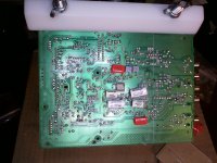
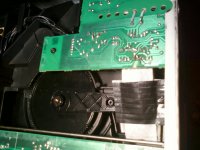
biggest issue is how to find where to make the break on the a150 board ?
Is there a way to find that same spot on pcb once removed say with a tester and follow traces?
is the line broken in between small and large transistors?
If I pulled the board and showed high res pictures of both sides and gave part numbers on arrows?
I know that`s a lot to ask so if you don`t want to get that far into it I understand.
does removing that fuse on pcb make any sonic difference?
and if I remove those fuse clips what if transformer or caps or rectifier craps out will that kill the amp?
just weighing the choices
thanks again for way more in depth help than I ever though I would get on ANY forum, and I have been on a few.
Glen
You are correct about your description of supply shunt caps. Yes, from supply rail to ground. For such a low voltage rail, i.e., +5V, I always use at least 1000uf at each supply pin, then 1-2uf of cheap, usually Panasonic, polyester film cap, then a small very nice film cap(0.022uf RT or a much larger "generic" styrene, such as Mial or Philips). On the pin that supplies the analog portion of the dac, I'd keep to the RT and possibly also add 0.1-0.33uf of a film/foil PP, a PPFA if there is room, or an SCR/Axon tinfoil/film if space is tight.
The rail fuses are a LARGE bottleneck to current delivery from the main caps. It's BAD enough that the main caps are so physically & electrically far away(I would set up banks of smaller lytics, adding up to as much or more cap value, right in front of each channel board), so the fuses are basically adding insult to injury, and the amp is reliably built enough to not worry about anything but the mains fuse. If anything blows up, it won't blow up any worse, as long as the mains fuse is not inappropriately increased in rating(i.e., may need to be higher to handle turnon surge if you go a lot larger on supply capacity, but only enough to never blow from that surge).
Even adding 1000uf on each rail for the input/pre-drive stages should make a pretty big difference in smoothness. I think 6800 would be a bit of overkill, which I am never against, but space may be a problem, and I would be perfectly ok with 4700uf or even 3300uf, as the early stages are not pulling a lot of current. Key thing is giving that added filtering some isolation from the output stage supply, via the wirewound resistors. I see that the schematic part reference numbers are different between DIA100 and A200, but I would be a bit surprised if the ref numbers for A150 were different than the A200, as the two models likely use the same channel boards. So, easiest thing is to look at the ref numbers I id'd & see if their positions by location & board traces seem to correspond to A200 diagram. For the caps, you don't need to use the "audio grade" Nichicons, as other grades like VR, VX, PF, PW, etc. will do just as well for the purpose once broken in & likewise bypassed with films.
You are correct about your description of supply shunt caps. Yes, from supply rail to ground. For such a low voltage rail, i.e., +5V, I always use at least 1000uf at each supply pin, then 1-2uf of cheap, usually Panasonic, polyester film cap, then a small very nice film cap(0.022uf RT or a much larger "generic" styrene, such as Mial or Philips). On the pin that supplies the analog portion of the dac, I'd keep to the RT and possibly also add 0.1-0.33uf of a film/foil PP, a PPFA if there is room, or an SCR/Axon tinfoil/film if space is tight.
The rail fuses are a LARGE bottleneck to current delivery from the main caps. It's BAD enough that the main caps are so physically & electrically far away(I would set up banks of smaller lytics, adding up to as much or more cap value, right in front of each channel board), so the fuses are basically adding insult to injury, and the amp is reliably built enough to not worry about anything but the mains fuse. If anything blows up, it won't blow up any worse, as long as the mains fuse is not inappropriately increased in rating(i.e., may need to be higher to handle turnon surge if you go a lot larger on supply capacity, but only enough to never blow from that surge).
Even adding 1000uf on each rail for the input/pre-drive stages should make a pretty big difference in smoothness. I think 6800 would be a bit of overkill, which I am never against, but space may be a problem, and I would be perfectly ok with 4700uf or even 3300uf, as the early stages are not pulling a lot of current. Key thing is giving that added filtering some isolation from the output stage supply, via the wirewound resistors. I see that the schematic part reference numbers are different between DIA100 and A200, but I would be a bit surprised if the ref numbers for A150 were different than the A200, as the two models likely use the same channel boards. So, easiest thing is to look at the ref numbers I id'd & see if their positions by location & board traces seem to correspond to A200 diagram. For the caps, you don't need to use the "audio grade" Nichicons, as other grades like VR, VX, PF, PW, etc. will do just as well for the purpose once broken in & likewise bypassed with films.
wow again and thanks, I think maybe I cooked my dac ic ha ha
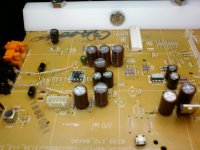
space was tight as you will see on pictures attached also a picture of power supply board I put esr tape on reg and bypassed 8000uf with a left over orange drop .22
any of these kill output on one channel dac ic?
heat and/or output from 2 prong soldering iron?
washing board with contact cleaner and blowing with dust off?
a continuity test on trace connected (farther down) to right channel output pin?
all of the above?
oh well if you are not prepared to break something, then you have no business messing with it in the first place!
just about to pull the trigger and order 3 from china but want to make sure thats it
I am getting sound left channel and I get ac from that dac pin also 2 volt dc from that pin
no sound on right channel, no ac on dac pin, no dc on dac pin for that channel.
gotta be dac no?
as for my silly cap question, I understand a little better now (ie.) only ac passes through cap (coupling) so to smooth dc it`s parallel or across the rails positive to negative or ground (also ground or chassis ground)
is that correct?
as for the acurus a150 I totally apreciate the time you have spent with me on this and I will attempt this.
so I will find something compact but decent spec cap (bypassed) 2 on each channel board wired with jump lead.
would occ 10g solid cryo romex work? or stranded better?
If I hold the board up to light I should see the traces and be able to follow, right?
whats the best way to break trace? drill board?
do resistors provide noise isolation? and will that limit current?
as for fuse I have not (yet) raised capacitance any more than 2000uf from stock plus whatever in films to bypass so stock slow blow will be fine.
(could not find any new 40000uf 100v anywhere unless I buy 10)
anyone know where to source these?
I noticed on schematic for dia 100 it is same for a250 just different rail volts
I also got a a200 skematic and it shows the number references like q17 are in the same place on schematic sooo...
I will order parts for that next maybe rewire with 12 gauge?
thanks again Stephen
PS if you ever get to calgary alberta canada I owe you beers and dinner
Attachments
Decoupling caps for digital are there to provide the instantaneous charge required when the logic state changes, the small the better and as near the power supply pins as possible, MLCC SMD ceramic are the best choice, these are then supplied by reservoir caps a bit further away from the power pins and so on back to the main reservoir caps and the PSU. For digital decoupling and anything else where near instant current is required inductance is the killer so leaded devices are no use for local decoupling at the pins. With todays logic switching speeds proper decoupling is becoming more critical.
Decoupling caps for digital are there to provide the instantaneous charge required when the logic state changes, the small the better and as near the power supply pins as possible, MLCC SMD ceramic are the best choice, these are then supplied by reservoir caps a bit further away from the power pins and so on back to the main reservoir caps and the PSU. For digital decoupling and anything else where near instant current is required inductance is the killer so leaded devices are no use for local decoupling at the pins. With todays logic switching speeds proper decoupling is becoming more critical.
ok I need to mention I`m a carpenter with very little electronics experience
when you say decouping for digital are you talking about vddd pin on dac ic or digital power supply to dac? I left the original .1uf smt and added 100uf 25v silmic replacing 47uf (original also silmic) and added vishay .022uf
lol I could only hear the left channel so I have not done any listening yet.
I somehow cooked right channel output on dac (I think)
leads on all power pins are very short like 3/16'' except on main power supply from tranformer which now has a .22uf bypassing main panasonic 8200uf (only one that would fit). I covered the leads with teflon tube but they are maybe 1'' long and on separate board from dac.
thanks for the reply
Glen
The best option is small MLCC SMD caps as near to possible to the digital supply pins on the DAC for the digital side, preferably via'ed down to a ground and power plane pair.
via`ed? power plain? you lost me
One lead goes to ground and one to power trace
is that what you mean?
Thanks Mooly, sorry didn't explain clearly, I will provide some pictures later as I,m just gonna commute home from work (London to Blackburn).
Impedance vs Frequency
The graph shown above is an important graph for decoupling capacitors, more detail later.
Impedance vs Frequency
The graph shown above is an important graph for decoupling capacitors, more detail later.
Thanks Mooly, sorry didn't explain clearly, I will provide some pictures later as I,m just gonna commute home from work (London to Blackburn).
Impedance vs Frequency
The graph shown above is an important graph for decoupling capacitors, more detail later.
thanks hey
I do not know the terminology but learning
Glen
This is quite a good basic explanation:
www.cvel.clemson.edu/presentation_slides/PowerBus-decoupling.pdf
SMD or surface mount devices mount directly to pads on the PCB, where as PTH components have leads that solder in to plated holes in the PCB. The advantage of SMD is no long lead out frame from the silicon to the PCB and thus reduced parasitic inductance. The problem with SMD devices is that they are getting smaller and smaller. The older devices are managable for DIYers (SOIC, 1206 0805 chip resistors and caps) but the newer devices (BGA's QFN's IC packages and 0402 0201 01005 chip devices) are hard enough to place and solder even with a full assembly line. This shrinking size, smaller features on the actual chip and reduced operating voltages is allowing ever increasing operating speeds at the expence of more critical layout and simulation of the layout for signal integrity and power delivery system dynamic impedances.
Decoupling is becoming more critical due to the increasing speed increase (signal rise times being the biggest problem), for most DIY though using older technology, standard good practice decoupling will suffice, just check the rise times (and fall time) of any device you are going to use.
This is a bit deeper but illustrate quite well the prinicples:
www.sigrity.com/papers/EMC-IEEE-BK/si_chapter.pdf
This text file is a list of some of the links to documentation I have collated relating to PCB layout, there are some good basic guides as well as more in depth info, hope it helps:
Finaly PCB design should be fun, if you get frustrated with part of the design, leave it for a while and do something else, then when you go back you can usually see the solution.
Attachments
This is quite a good basic explanation:
www.cvel.clemson.edu/presentation_slides/PowerBus-decoupling.pdf
SMD or surface mount devices mount directly to pads on the PCB, where as PTH components have leads that solder in to plated holes in the PCB. The advantage of SMD is no long lead out frame from the silicon to the PCB and thus reduced parasitic inductance. The problem with SMD devices is that they are getting smaller and smaller. The older devices are managable for DIYers (SOIC, 1206 0805 chip resistors and caps) but the newer devices (BGA's QFN's IC packages and 0402 0201 01005 chip devices) are hard enough to place and solder even with a full assembly line. This shrinking size, smaller features on the actual chip and reduced operating voltages is allowing ever increasing operating speeds at the expence of more critical layout and simulation of the layout for signal integrity and power delivery system dynamic impedances.
Decoupling is becoming more critical due to the increasing speed increase (signal rise times being the biggest problem), for most DIY though using older technology, standard good practice decoupling will suffice, just check the rise times (and fall time) of any device you are going to use.
This is a bit deeper but illustrate quite well the prinicples:
www.sigrity.com/papers/EMC-IEEE-BK/si_chapter.pdf
This text file is a list of some of the links to documentation I have collated relating to PCB layout, there are some good basic guides as well as more in depth info, hope it helps:
Finaly PCB design should be fun, if you get frustrated with part of the design, leave it for a while and do something else, then when you go back you can usually see the solution.
thanks again for the links and info, I havent had time to read them all yet, but will soon
I think I may buy a introduction to electronics or pdf book as a beginners guide
any recommendations?
trying to spend some time with girlfriend before dac arrives from china and I have to de-solder and re-solder new dac any tips on smd soldering?
watched a couple of vids on youtube but mainly they just make me want a soldering station
will a 2 prong soldering iron harm a dac chip?
thanks again to Stephen, Marce and Mooly
Glen
The art of electronics:
Amazon.co.uk: art of electronics 3rd edition: Books
The standard basic tome.
Amazon.co.uk: art of electronics 3rd edition: Books
The standard basic tome.
I have to de-solder and re-solder new dac any tips on smd soldering?
watched a couple of vids on youtube but mainly they just make me want a soldering station
will a 2 prong soldering iron harm a dac chip?
thanks again to Stephen, Marce and Mooly
Glen
Practice on something first. A 2 prong
") (you mean a double insulated non grounded iron) should be OK if it is designed for electronic use and has low leakage. Always make sure the equipment you are working on is totally disconnected from the mains.
(you mean a double insulated non grounded iron) should be OK if it is designed for electronic use and has low leakage. Always make sure the equipment you are working on is totally disconnected from the mains.http://www.diyaudio.com/forums/parts/127924-working-smd-how-do-without-specialised-tools.html
Practice on something first. A 2 prong
http://www.diyaudio.com/forums/parts/127924-working-smd-how-do-without-specialised-tools.html
thats good to hear because I don`t really want to spend 130 for a hakko yet
I was looking online and they have a low heat solder that will de-solder with ease?
ever tried that?
thanks
Glen
I've never used low meting point solders for electronic work but any decent iron should have no problem with "normal" solders. I don't use lead free either for home stuff
just watched a good demo
Surface Mount Soldering 101 - YouTube
called chip quik (solder & bismuth) for clean removal of smd type
this was good too
Professional SMT Soldering: Hand Soldering Techniques - Surface Mount - YouTube
thanks
Glen
Best advice has to be to practice on something first.
I think a lot will come down to what you feel comfortable working with. I used to have use of a PACE surface mount rework station years ago and also a METCAL RF soldering iron but always found I prefered my own methods. Its what you get used to.
Get some old remotes and have a go on those
I think a lot will come down to what you feel comfortable working with. I used to have use of a PACE surface mount rework station years ago and also a METCAL RF soldering iron but always found I prefered my own methods. Its what you get used to.
Get some old remotes and have a go on those
- Status
- This old topic is closed. If you want to reopen this topic, contact a moderator using the "Report Post" button.
- Home
- Source & Line
- Digital Source
- help needed dc coupling ,is there a better way?