I am attempting to build a DAC with 8x oversampling, ASRC, and balanced AD1865 DAC's.
The setup is like this:
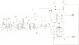
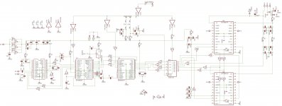
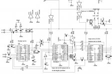
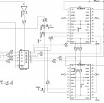
CS8414 (Decode SP/DIF convert to I2S) -> AD1896 (Reduce Jitter/Resample everything to 44.1KHz (fed with 11.2896MHz super clock)) -> SM5842 (Oversampling filter fed with super clock) -> flip-flop (resample with super clock) -> 2x AD1865 (one supplied with L data and inverted L data, to create balanced outputs). This setup makes sense to me, advice would be greatly appreciated. I don't know if the AD1896 will communicate with the SM5842 as the data sheets say different thing's (right justified = LSBJ)??? Is the Flip-flop necessary to reduce jitter or could it be replaced with a inverter to get the inverted data signals for the DAC's?
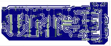
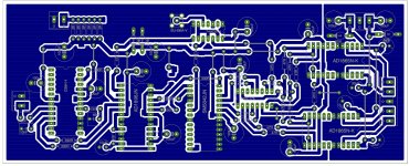
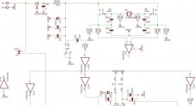
I created a PCB layout with clock on separate PCB. I am not a DAC/PCB expert so advise on the layout would be greatly appreciated.
http://www.dddac.de/files/SM5842.pdf
http://www.analog.com/static/imported-files/data_sheets/AD1896.pdf
http://www.analog.com/static/imported-files/data_sheets/AD1865.pdf
http://www.jitter.de/pdfextern/8413-4.pdf
http://www.fairchildsemi.com/ds/MM/MM74HC175.pdf
http://cds.linear.com/docs/Datasheet/1963fc.pdf
The setup is like this:
CS8414 (Decode SP/DIF convert to I2S) -> AD1896 (Reduce Jitter/Resample everything to 44.1KHz (fed with 11.2896MHz super clock)) -> SM5842 (Oversampling filter fed with super clock) -> flip-flop (resample with super clock) -> 2x AD1865 (one supplied with L data and inverted L data, to create balanced outputs). This setup makes sense to me, advice would be greatly appreciated. I don't know if the AD1896 will communicate with the SM5842 as the data sheets say different thing's (right justified = LSBJ)??? Is the Flip-flop necessary to reduce jitter or could it be replaced with a inverter to get the inverted data signals for the DAC's?
I created a PCB layout with clock on separate PCB. I am not a DAC/PCB expert so advise on the layout would be greatly appreciated.
http://www.dddac.de/files/SM5842.pdf
http://www.analog.com/static/imported-files/data_sheets/AD1896.pdf
http://www.analog.com/static/imported-files/data_sheets/AD1865.pdf
http://www.jitter.de/pdfextern/8413-4.pdf
http://www.fairchildsemi.com/ds/MM/MM74HC175.pdf
http://cds.linear.com/docs/Datasheet/1963fc.pdf
Attachments
Last edited:
Yes, you need DFF. Otherwise the jitter will suffer badly.
- Replace the CS8414 to something better, WM? Then you'll need to care 'bout 3.3-5v CMOS translation.
- Your clock distribution is bad. Check transmission lines.
In general - impedance control, single active source for every IC input.
That means:
- no jumpers
- need clock buffers (buffers or inverters - from fast logic family, not AC)
- reflection-suppressing resistors are at transmitter side.
- solid ground plane under clock's traces
- coax from clock PCB to DAC pcb
ASRC... is doubtful.
>>So I should add buffers to the clock lines & extend the ground plane around the clock trace?
Yes.
You'll have to control the impedance of traces.
With thick boards this is less easy, as your ground plane is far away of your traces.
Use Saturn PCB calculator to calculate trace impedances. With 2-sided board you have 2 choices - classic stripline - a conductor over ground plane. And coplanar waveguide - a conductor on ground plane + tightly surrounded by ground planes.
Stripline is better controlled, but requires thin board or too wide trace.
Coplanar thing is less controllable, requires precise spacing between ground plane surrounding, and tightness of 7-8mil conductor to ground plane spacing.
>>Should I remove the flip flop and just use an inverter to get the out of phase data signals.
No, you need DFF (D flip flop). It's called "reclocking". And by using 74HC175 you get inverted data for free.
>>As the output of the ad1896 should already have low jitter?
Somewhat ok jitter. Then you throw it's output to DF (digital filter) - that adds some jitter.
You want to have the jitter as low as possible. Simplest way of doing this is to "reclock" - then you'll have the jitter of clock + traces + maybe a buffer + DFF.
The less is in between, the less jitter you'll have.
You have 2 ICs that require low jitter thing.
1. DACs.
2. ASRC.
Draw a clocking block-scheme of your circuit. Circle the important traces, take care of them.
The rest is less important.
Then you'll need to be aware of EMC (electromagnetic compartability).
Rules of thumb - keep digital traces short, keep solid ground plane under these traces (no cutouts, no crossing traces).
Throw a ferrite bead on every digital IC PSU: PSU trace > Ferrite bead (near the IC) > IC Vcc ping > capacitor to ground.
Make sure you have smooth, solid, short ground plane from the grounded capacitor pin to GND pin of IC.
From external source /connector/, "superclock" of some sort.
Okay.
What is your plan for the analog stages?
Last edited:
I plan on using 4 pass d1 Iv stages with fet ccs's and pass b1 buffer.
The AD1865 is one of the few DAC chips which can be used with a sizable passive resistor for I/V conversion. Among the reasons your thread caught my eye is that one of my experimental DACs features the CS8416 + AD1896 + AD1865. In that DAC I utilize 330 Ohm passive I/V resistors followed by capacitive coupling directly to my JFET preamp - with no intervening active analog circuitry in the DAC. The resulting sound is very transparent.
The AD1865 is one of the few DAC chips which can be used with a sizable passive resistor for I/V conversion. Among the reasons your thread caught my eye is that one of my experimental DACs features the CS8416 + AD1896 + AD1865. In that DAC I utilize 330 Ohm passive I/V resistors followed by capacitive coupling directly to my JFET preamp - with no intervening active analog circuitry in the DAC. The resulting sound is very transparent.
How to you like the ad1896? Will the ad1896 convert any input sample rate into the master clock freq. (11.2896mhz) divided by 256 = 44.1KHz? Is your setup nos or os? Could you post schmatics of the circuit your dac uses? What power supplies do you use for the dac (i plan to use 7 salas shunts)?
Last edited:
benproiii: Do your homework. Study the datasheets.
The 7404 is TTL and will not drive CMOS. 7404 Voh=2.4v, SM5842 Vih=3.5v.
A real clock driver is preferred over random gates from any logic family.
All your fancy components will be wasted without the foundation of a well-crafted, multi-layer PCB.
The 7404 is TTL and will not drive CMOS. 7404 Voh=2.4v, SM5842 Vih=3.5v.
A real clock driver is preferred over random gates from any logic family.
All your fancy components will be wasted without the foundation of a well-crafted, multi-layer PCB.
I was going to use this inverter http://www.onsemi.com/pub_link/Collateral/74HC04.REV1.PDF which says it supports CMOS.
Which clock driver IC would you recommend?
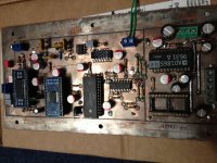
I cannot make Double sides boards with the supplies I have, i have seen many high speed digital electronics with single sides boards and they seem to work fine. Which methods should I use to optimize the single sided ground plane?
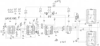
I uploaded the latest circuit (i switched to SMD .22uF ceramic decoupling caps, added 5.6v zener's across rails to protect from over voltage ) (The jumpers going from the power rail's to the IC's have ferrite beads on them)
What type of decoupling caps do you recommend for the 100uF's OSCONS,MUSE?
Which clock driver IC would you recommend?
I cannot make Double sides boards with the supplies I have, i have seen many high speed digital electronics with single sides boards and they seem to work fine. Which methods should I use to optimize the single sided ground plane?
I uploaded the latest circuit (i switched to SMD .22uF ceramic decoupling caps, added 5.6v zener's across rails to protect from over voltage ) (The jumpers going from the power rail's to the IC's have ferrite beads on them)
What type of decoupling caps do you recommend for the 100uF's OSCONS,MUSE?
Attachments
How to you like the ad1896? Will the ad1896 convert any input sample rate into the master clock freq. (11.2896mhz) divided by 256 = 44.1KHz? Is your setup nos or os? Could you post schmatics of the circuit your dac uses? What power supplies do you use for the dac (i plan to use 7 salas shunts)?
I found the AD1896 to be very useful. I used it as the digital interpolation filter in my DAC. As such, I was able to experiment with OS, NOS, and linear phase apodizing. The AD1896 utilizes an FIR linear (poly)phase low-pass filter as part of the sample rate conversion function, enabling OS. The sample rate function, and therefore the FIR filter, can be bypassed enabling NOS. The FIR low-pass corner frequency can be 'programmed' to deliver an in-band linear phase apodizing cut-off frequency.
I'm not sertain what you are asking here: "Will the ad1896 convert any input sample rate into the master clock freq. (11.2896mhz) divided by 256 = 44.1KHz?"
This DAC was designed purely for experimentation. I don't think the schematic would be of much use to another diy'er. I'm not being coy here, just nothing world shaking about that design. For example, I used a 7808 and a 7908 as primary regulators, followed by cascaded LDO secondary regulators. I wasn't using this particular experimental DAC for exploring regulator solutions.
Last edited:
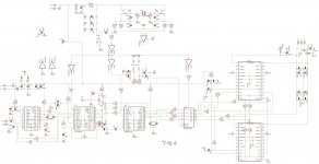
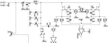
I just found some double sided copper clad, I'm going to try the double sides design, this is what I came up with. I included the clock onboard, with separate PSU. I have a question about the oscillator, how much heat does the U309 dissipate? because it's a SOT-23 package and I don't want it to overheat.
design suggestions would be appreciated.
design suggestions would be appreciated.
Attachments
Last edited:
Im not sure if about the chips reset pin should the AD1896's reset pin be tied to the SM5842's reset pin so they turn on at the same time?
how will the clock sync with the AD1896, SM5842, 74HC175? what happens if the clock does not turn on, will the chips like blow up?
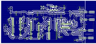
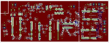
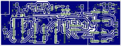
how does the new PCB look? (double sided)
how does the clock look, do you think it will have low jitter?
If I play a 96K file on this DAC will the AD1896 convert it into 44.1KHz 16-Bit?
Are there any bugs in these chips I should know about (wired noises on turn on, no signal)?
how will the clock sync with the AD1896, SM5842, 74HC175? what happens if the clock does not turn on, will the chips like blow up?
how does the new PCB look? (double sided)
how does the clock look, do you think it will have low jitter?
If I play a 96K file on this DAC will the AD1896 convert it into 44.1KHz 16-Bit?
Are there any bugs in these chips I should know about (wired noises on turn on, no signal)?
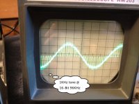
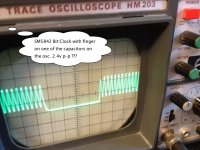
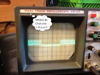
I built the PCB for this DAC and I cannot get it to work with any input frequency above 48KHz (it outputs weird pulsating sine waves) I thought it was something to do with the clock but I hooked it to a normal 11.2896MHz pierce oscillator and it still does the same thing. This circuit has been acting super weird if I touch the colpitts capacitors on the oscillator the pulsating oscillations move a little, and the amplitude of the bit clock to the DAC increases from 1v p-p to 2v p-p.
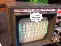
I also had to disable the reclocking circuit it won't allow the bit clock to flip flop throughout it. I tried inverting the clock signal to it and it does nothing. I attached an image of the bit clock coming out of the SM5842, should it be a square wave?
could some one please help me analysis this circuit to help me find out what I did wrong?
There are no shorts or open circuits on the board, I tried to use chemical tinning on the board and it tarnished.
Attachments
Last edited:
- Status
- This old topic is closed. If you want to reopen this topic, contact a moderator using the "Report Post" button.
- Home
- Source & Line
- Digital Source
- Balanced, 8XOS, ASRC, AD1865 DAC