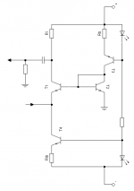
Here is an idea I had for those of you who want to try something a little different in your DAC/CD output stage. Take a look at the schematic which is attached. Basically it is a common base amplifier used as an I/V stage suitable for PCM1702/1704/63 or similar current output style DACs. This is STILL VERY MUCH A SKETCH at the moment but I thought some of you may wish to have a play and tweak it.
T1 forms the actual gain transistor and I suppose it can be considered the only transistor in the signal path. T2 creates a voltage reference for T1s base. T3 and T4 form constant current sources the current through these should be nearly identical.
The emitter of T1 will provide a low impedance point for the DAC chip. The DC voltage at this point will probably need trimming to zero by a pot arrangement around Rib enabling you to vary the bias current through T1 either side of the current level set by fixed current source T3.
I am not sure what the bias current should be but I would say that 10mA would be a good starting point.
Ri is where the actual I/V conversion takes place and the value chosen for this resistor is a direct compromise between output level and output impedance. Its fairly clear to see that its value is the output impedance. The maximum output level (RMS) of the circuit is equal to the maximum RMS current from the DAC chip multiplied by the value of Ri. For example if it is being used with say a PCM1704 (1.2mA) peak and Ri=1K then the maximum drive level is 0.8485v RMS with an impedance of 1K. Clearly this is not your usual CD Player drive but should be suitable for amplification by a good pre-amp, a ZEN for example.
It will be important to watch the voltage drop across Ri to ensure that T1 has an adequate Vce drop, you may need to raise the supply voltage. Speaking of supply it will have to be very well filtered as any noise on the positive supply will appear at the output.
Lastly this design has a very wide bandwidth and digital noise will be passed through to the output. The bandwidth can be decreased by adding a capacitor across Ri. There is lots of room for experimentation here and results will probably vary for different amplifiers and systems.
I would really like some opinions on this so let me know what you think.
Attachments
Ha, you'er a genius if you had never knew the current mode technology.
Yes, it's a good idea, but it isn't prefect.
1. There're tow LEDs which be used in constant current source. It will caused un-match current between these two CCS. In this case, the collect current of T1,T2 must be matched.
2. The rbb1, rbb2 will cause high distortion. rbb is resistance of base area of transistor. You may needed to generate a negative resistance to reduce it's affort.
3. You may needed to add a low pass filter to reduce noise.
4. You may needed to add a output buffer to iso this stage, so it can reduce distortion. The output impendance of this stage is Ri // Rload_impendance.
My english is not well. I hope that you can understand what thing i want to say.
hill thanks for your info.
I ran some quick simulations in the multisim 2001 demo and came up with the following
THD was around 0.0035%
This was obtained under the following conditions.
T1 & T2 were 2N2222s. Input current 1.2mA peak (2.4mA p-p ie. full drive of PCM1704/2) at 10KHz analyzed up to the 9th harmonic. Bias current = 10mA, Ri = 1K and the supply rails were +/- 20v.
Of course the output of the DAC was assumed to be a perfect current source so I decided to change the model for a voltage source in series with a 1K resistor - the output of the voltage source was 2.4v p-p.
The THD was now 0.0055%
The impedance at the emitter of T1 is roughly 3.5 ohms but clearly this is not resistive but even so the above voltage source/ resistor demostration shows that it may not affect THD at the output that much.
The bandwidth, around 40MHz. This can be greatly decreased by a capacitor in parallel with Ri. In this case 3nF in parallel with 1K gave a bandwidth of about 50KHz.
What about this one ?
Hi,
Reminds me of something I thought of a few years ago. Basically, it's a common gate mosfet, followed by a buffer (Thanks Nelson for the idea") ).
).
The Jfet diff pair is here to maintain the source of M1 (i.e. the current input) at 0V. In a previous version, I used a BJT diff pair, but I'm not sure how the base currents drawn by the BJTs would affect the I/V conversion...
I really enjoy the previous version (with PCM63), but want to try this "new" version (differences are the Jfets instead of BJTs, and a DC servo at the output). May be I will try it with a cascoded output instead of the simple buffer stage.
Any comments welcome
Hi,
Reminds me of something I thought of a few years ago. Basically, it's a common gate mosfet, followed by a buffer (Thanks Nelson for the idea
). The Jfet diff pair is here to maintain the source of M1 (i.e. the current input) at 0V. In a previous version, I used a BJT diff pair, but I'm not sure how the base currents drawn by the BJTs would affect the I/V conversion...
I really enjoy the previous version (with PCM63), but want to try this "new" version (differences are the Jfets instead of BJTs, and a DC servo at the output). May be I will try it with a cascoded output instead of the simple buffer stage.
Any comments welcome
Attachments
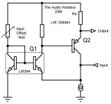
Both those look like nice designs the one by JM Didden seems to apply a simple feedback loop around the whole stage.
ftorres,
Do you know how similar your one is to the Passlabs D1 DAC?
I have also been throwing ideas around similar to your 2SK389 approach to maitain 0v at the source of the I/V MOSFET. In my current DAC I am using a OP-AMP setup as a DC Servo with a very low cut off frequency to eliminate feedback at audio frequencies. Your approach however will apply feedback around the MOSFET at audio frequencies and thus lower the impedance seen by the DAC chip.
Dave,
Yep, that's what I had in mind when I began to think of it I'm not quite sure the whole design is the same, since I never had the opportunity to approach a D1
Concerning the feedback, I must admit it's a question I asked myself (and not answered it...) : Is it better to have the Mosfet source all the time at 0V, or just to have a kind of DC servo as you use, only to correct the long term drifts (very low frequencies) of the Mosfet, just like at output ? Have you tried both ?
Concerning you last question, I'm sorry, but I don't exactly understand what you mean (my english's too bad ) Can you please elaborate ?
P.S. : I tested Didden's design long ago, but found it hard to stabilize (slow drifts). Surely some additionnal servo-type feedback will help, will try to re-test it.
Do you know how similar your one is to the Passlabs D1 DAC
Yep, that's what I had in mind when I began to think of it
I'm not quite sure the whole design is the same, since I never had the opportunity to approach a D1 Concerning the feedback, I must admit it's a question I asked myself (and not answered it...) : Is it better to have the Mosfet source all the time at 0V, or just to have a kind of DC servo as you use, only to correct the long term drifts (very low frequencies) of the Mosfet, just like at output ? Have you tried both ?
Concerning you last question, I'm sorry, but I don't exactly understand what you mean (my english's too bad
) Can you please elaborate ?P.S. : I tested Didden's design long ago, but found it hard to stabilize (slow drifts). Surely some additionnal servo-type feedback will help, will try to re-test it.
Ftorres,
Great design! We need more of this stuff on the site.
Looks similar to the Pass design but with the addition of the servo. I would probably capacitor couple the output stage and leave out the servo if I built it.
Do you have a board layout by any chance?
Jam
P.S. I wonder if Grey will notice you liberal use of current sources in the design.
Dave,
Ok, much more clear to me
Well, I just have simulations results for this one using demo version of Micro-Cap, an it gives me +/-0.1mV (100uV) at the source of M1 (provided the spice models are accurate ).
And it fits what I had measured on my previous version, where I use a MAT02 for the diff pair, and I was just at the noise level of my DMM.
Jam,
Thanks for your kind comments. Concerning PCBs, not for the moment, but I'll have to develop one for testing, and I'll sure post it. You can try it without servo, just making a CCS as the others. But I dont think you really need a cap. I the version I currently use (as in the one), the variable source resistor of M2 lets you null the output offset with a good accurracy (about 10-15 mv if memory serves). The servo is just here to account for thermal drifts in the circuit.
And yes, I like active current sources. With all the Leds glowing, I find it prettier. It has a "tube" feeling when you Dac glows in the dark
Ok, much more clear to me
Well, I just have simulations results for this one using demo version of Micro-Cap, an it gives me +/-0.1mV (100uV) at the source of M1 (provided the spice models are accurate
). And it fits what I had measured on my previous version, where I use a MAT02 for the diff pair, and I was just at the noise level of my DMM.
Jam,
Thanks for your kind comments. Concerning PCBs, not for the moment, but I'll have to develop one for testing, and I'll sure post it. You can try it without servo, just making a CCS as the others. But I dont think you really need a cap. I the version I currently use (as in the one), the variable source resistor of M2 lets you null the output offset with a good accurracy (about 10-15 mv if memory serves). The servo is just here to account for thermal drifts in the circuit.
And yes, I like active current sources. With all the Leds glowing, I find it prettier
. It has a "tube" feeling when you Dac glows in the dark My design.
It's working in my DAC which is used PMD-200+2PCM1704K.
For your reference.
My MSN: aax_man@hotmail.com
It's working in my DAC which is used PMD-200+2PCM1704K.
For your reference.
My MSN: aax_man@hotmail.com
Attachments
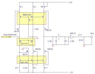
Nice design hill.
I had not heard of the ALD1102 before, I took a look at the datasheet and it seems perfect for the Job. Who is the distributor?? I am also suprised we don't see it in amplifier
front-ends more often.
Also how did you manage to get hold of a PMD200??
Cheers,
Dave
I had not heard of the ALD1102 before, I took a look at the datasheet and it seems perfect for the Job. Who is the distributor?? I am also suprised we don't see it in amplifier
front-ends more often.
Also how did you manage to get hold of a PMD200??
Cheers,
Dave
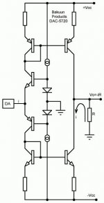
Bakuun Products, used this circuit in the early 90s
They now make a Chip for thier Amps, DAC, etc. and for DIY, its more commonly called the Satri-IC.
<a href="http://www.tachyon.co.jp/bp/bp.html"><img src="http://www.tachyon.co.jp/~sichoya/bpkit/5511kparts/product/satri-ic.jpg"></a>
The pic will take you to Bakuun Products english page, <a href="http://www.tachyon.co.jp/~sichoya/">Here will take you to Tachyon</a>
The chip is a bit more developed than this early circuit, the power amp article I have in MJ shows all the current sources doubled up.
Regards
James
- Status
- This old topic is closed. If you want to reopen this topic, contact a moderator using the "Report Post" button.
- Home
- Source & Line
- Digital Source
- CD/DAC Output Stage for Purists