Hi,
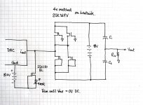
remark: There´s a small failure in #182.
It reads: Trim until Vout=0Vdc.
It should read: Trim until the voltage at the input of the I/V stage is 0Vdc, or(!) till the supply voltages measured against Vout are symmetric +-0.5*Vsupply (here: +-9V)
Since the trimming is temperature sensitive, give the circuit plenty of time to warm up and settle at a stable temperature.
jauu
Calvin
Hi,
C1 and C2 keep the output DC-free anyway. A current asymmetry at the input will lead to an input offset voltage and to a asymmetry of the JFETs supply voltage potentials.
Especially with the CEN the input offset voltage is quite small, within a couple of mV. The supply potential asymmetry on the other hand may reach several volts and one supply potential may even become smaller than the needed signal voltage swing --> clipping. Supply potential symmetry is therefore a good indicator for trimming. With proper trimming the supply voltage may be reduced, thereby reducing power dissipation (only sensible, if heat dissipation is a problem, since lower supply voltage increases THD).
jauu
Calvin
Last edited:
Hi,
right Kirchhoffs law applies, but a cap doesn´t conduct at DC. Only the AC signal current ´passes´ the caps and generates a signal voltage over Riv The trimming is done without signal under DC-conditions.
The 560Kohm resistors shown in the earlier sketches supply for a dc-current-path though and a positive dc-offset voltage over Riv occurs.
The Input of the stage will also be pulled into positive direction and eventually the protection diodes of the DAC will start conduction, thereby limiting the offset at the input to the Vf of the diodes. The positive potential of the supply voltage will be approx. the supply voltage, the negative supply potential will be at approx. Vf.
The bipolar version is more forgiving in this respect and creates lower offsets from the start. Anyway, the variations in the symmetry of the supply line potentials are the most sensitive indicator for trimming.
jauu
Calvin
> Anyway, the variations in the symmetry of the supply line potentials are the most sensitive indicator for trimming.
We agree on that.
It is also why I mentioned in post #170 to trim offline using a multimeter first before fine trimming in circuit.
Also for trimming one might lower the 560k resistors to 2k temporary, and remove them once done.
Patrick
We agree on that.
It is also why I mentioned in post #170 to trim offline using a multimeter first before fine trimming in circuit.
Also for trimming one might lower the 560k resistors to 2k temporary, and remove them once done.
Patrick
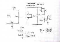
Thanks!I have been asked to publish a schematics of SEN in combination with the likes of ES9018, PCM1794, 1798, etc., as descrived in post #170.
Here you are. Hope this makes it clear.
It looks like the very same Sen, only with a current bias circuit. Does it mean one can use Cen the same way?
I don't quite understand how to power this constant current source properly. How separate must it be? Is it possible to use the same power supply that powers I/V?
BTW, what is the acceptable voltage range for I/V? 18V isn't too practical, 15V or even 12V would be better...
Last edited:
> It looks like the very same Sen, only with a current bias circuit. Does it mean one can use Cen the same way?
Yes, but you probably might want to try using 2 pairs of JFETs instead of 1.
> I don't quite understand how to power this constant current source properly.
> How separate must it be?
Totally separate, as drawn. i.e. Separate battery required.
> Is it possible to use the same power supply that powers I/V?
Not for SEN / CEN.
Patrick
.
Last edited:
> Are you suggesting that its possible to do this with SEN/CEN?
Absolutely NOT.
SEN / CEN have floating supplies that swing with the output signal.
But you can think of a way to use e.g. the analog supply of the DAC and some additional circuit to provide that voltage.
Patrick
Absolutely NOT.
SEN / CEN have floating supplies that swing with the output signal.
But you can think of a way to use e.g. the analog supply of the DAC and some additional circuit to provide that voltage.
Patrick
Note that the schematics posted in post #182 only applies to ES9018 when use in stereo mode.
If you want to use ES9018 as 4 or 8 channel, I think it is wise to apply voltage offset (Vcc/2, or 1.65V for 3.3V supply).
As mentioned above, this is best taken off the analog supply of the DAC.
In that case (4 or 8 channel), the normal SEN / CEN circuit applies.
No need to increase no of FETs or Idss.
You may (ideally but not necessarily) wish to keep Vds of both top & bottom JFETs identical when applying this offset voltage to the JFET gates.
In that case, you should change R1 & R2 such that
R1 / R2 = (18V/2 + 1.65V) / (18V/2 - 1.65V) = 1.45
Keeping R1 at 560k, R2 should be changed to 390k.
Patrick
.
Last edited:
Understood.Totally separate, as drawn. i.e. Separate battery required.
What about the Sen/Cen power voltage? How far can I lower it without considerable loss in characteristics?
> BTW, what is the acceptable voltage range for I/V? 18V isn't too practical, 15V or even 12V would be better...
Minimum 15.6V (min 5V Vds for each FET plus 5.6v pk-pk swing), maximum 25V (limited by Vgds of 2SJ74).
For SEN, you might go further to 36V if you so wish.
If you lower it further, you increase distortion significantly due to non-linear JFET capacitances at low Vds.
The higher the voltage, the lower the capacitances, the lower the distortion.
Patrick
.
Last edited:
Seems that there are quite a few 9018 owners out there not entirely happy with their own IVs.
As requested attached a schematics for the 9018 operating in Voffset mode.
Shown here as used for 4 or 8 channels.
For stereo double the number of JFETs (in case of SEN use 4x 2SK369 as posted in #182.
Disclaimer :
I have not built this, nor do I intend to in the coming months.
Patrick
As requested attached a schematics for the 9018 operating in Voffset mode.
Shown here as used for 4 or 8 channels.
For stereo double the number of JFETs (in case of SEN use 4x 2SK369 as posted in #182.
Disclaimer :
I have not built this, nor do I intend to in the coming months.
Patrick
Attachments
- Home
- Source & Line
- Digital Line Level
- Zen -> Cen -> Sen, evolution of a minimalistic IV Converter