Isn't the mother project (sdr-widget) mostly about capture?
I suppose but it would be nice to have the capture in the AW. More I2S ports or spdif etc.
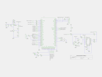
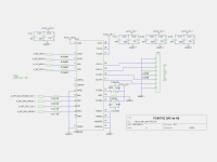
PCM1792 AB board
I have been working on an AB board based on the PCM1792 chip and Borge's USB-I2S module. I would like to experiment with different I/V stages, so my output is the balanced current out with reference voltages. (I have the Nelson Pass D1 I/V section already and I will also build this: http://www.diyaudio.com/forums/diyaudio-com-articles/172983-zen-i-v-converter.html )
For the voltage regulators on the non-USB side, I have decided to use Demian's series-regulator section instead of the shunt version. I might play around with the shunt version later.
GPIO for SPI The PCM1792 DAC chip needs to be controlled through SPI, so I am planning on modifying the widget code to send SPI initialisation codes. However, I have not yet spent any quality time with the widget code - does anyone know if it is a poor choice to use GPIO 6,7,9 and 10 for the SPI?
Attached it is the schematics and my layout - please comment, if you have any suggestions. The size is 10x10 cm so that I can use one of the batch pcb-manufactures.
Attachments
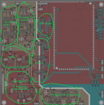
I think that board is really interesting. Would it be possible to bring the ADC lines out to a header (62,64,66, clocks and grounds)? There is a lot of interest in a capture variant. Perhaps Borge can comment.
One thing to be very careful of is the loop around a current output DAC. That link is very sensitive to external magnetic fields. it cannot tell a different between internal currents and induced currents. If the peak current is 10 mA then -120 dB is 10 nA, not very much. I would make that extremely small and using an airplane board would be a good idea (to keep the currents at orthogonal to any others in the system).
One thing to be very careful of is the loop around a current output DAC. That link is very sensitive to external magnetic fields. it cannot tell a different between internal currents and induced currents. If the peak current is 10 mA then -120 dB is 10 nA, not very much. I would make that extremely small and using an airplane board would be a good idea (to keep the currents at orthogonal to any others in the system).
1. I think that board is really interesting. Would it be possible to bring the ADC lines out to a header (62,64,66, clocks and grounds)? There is a lot of interest in a capture variant. Perhaps Borge can comment.
2. One thing to be very careful of is the loop around a current output DAC. That link is very sensitive to external magnetic fields. it cannot tell a different between internal currents and induced currents. If the peak current is 10 mA then -120 dB is 10 nA, not very much. I would make that extremely small and using an airplane board would be a good idea (to keep the currents at orthogonal to any others in the system).
Thanks for your comments!

1. A header to capture sounds easy, especially if it can be handled in the digital part - I am just reluctant to put too much stuff on the clock in the analog section.
2. Good point about the currents. Sorry for my ignorance, but what is an "airplane board"?
Airplane board- a board "floating" above the main board on a connector. If its perpendicular to the main board its even better.
The capture part of this board would need the master clock to be in sync. The capture card could be a slave to the host and the clocks would come from the digital section.
The capture part of this board would need the master clock to be in sync. The capture card could be a slave to the host and the clocks would come from the digital section.
I have been thinking a lot about this - but not reached a conclusion. Perpendicular airplane board is probably not going to fly, because some of the components I was thinking about putting on the IV stage are bulky... how is the common mode rejection typically on current out dacs? Couldn't the issue be solved by routing the diff pair close and ensure nearby gnd return path?
how is the common mode rejection typically on current out dacs?
Nonexistant. . .
The common mode rejection comes from the next stage. For a current out DAC the next stage needs to create a virtual ground at the output node. A reference would come from the dac as well. The area inside that loop will be sensitive to interference. Also keep in mind how fast the current needs to slew. That calculation which needs to include the out of band energy at the output pins is the biggest challenge. If yopu ignore it the current will go somewhere, possibly charging caps and active device nodes waiting to discharge. This is all before the image rejection filter. You could add a passive filter at the DAC output but that would adversely impact the VI stage if its source Z is increasing. Lots of interesting experiments possible.
OT:
I'm actually struggling with the same kind of issues these days. Laying out a new OPA1704 IVC I spend 10x the time looking at where the current goes as I do actually connecting the thing. And when currents are conserned I spend 10x the time considering a return current than I spend on the actual intended currents. Too many designers believe slapping on a ground plane or two at the end will do the trick.
Børge

Not sure if I see pink and green loops, could you link to the actual layout again?
When I design analog parts my checklist tends to be something like this:
1 - Place decoupling caps with the smallest value closest to the load, place increasingly larger caps more and more peripherally
2 - Minimize the loop made up of chip's ground pin (of relevant analog or digital domain), chip's power pin and the two pins on the decoupling
3 - Make sure there is very good ground conductance underneath the chip with all ground pins connected both toward decopling on the outside and the ground plane underneath it
4 - Try to route power to the peripheral largest caps in the decoupling stack associated with each loa pin
5 - Move blocks of chip+decoupling around to minimize the loop area of any signal correlated current.
6 - Signal correlated current doesn't just appear. It comes out of the decoupling cap, flows into the chip's power pin, through an internal driving resistor and then out the output pin. That same current may be consumed by an op-amp output somewhere.
7 - Whenever I get lost in this I model my chip outputs as variable voltage sources between power pin and output pin and draw the full schematic of decoupling and analog signals.
... or you may just say screw it, pour the ground plane and pour yourself a drink
Børge

I haven't really separated DAC and IVC like that in any of my designs. At least have ground on either side of the track pair (in the plane) and below them on the board. Make sure that ground is well connected to the ground underneath the IC (ref.prev.msg.)
Now I understand Demian's point a lot better. Anything induced into a loop between A+ and A- will appear amplified on your output. High-frequency noise may be demodulated by non-linearities in following stages.
Some times it helps to read up on how people build radios, and then do the opposite
Børge
I haven't really separated DAC and IVC like that in any of my designs. At least have ground on either side of the track pair (in the plane) and below them on the board. Make sure that ground is well connected to the ground underneath the IC (ref.prev.msg.)
Now I understand Demian's point a lot better. Anything induced into a loop between A+ and A- will appear amplified on your output. High-frequency noise may be demodulated by non-linearities in following stages.
Some times it helps to read up on how people build radios, and then do the opposite
Børge
Lol
I used to say that too. But now I think following RF rules will take someone a long way.
Try treating ever trace as a transmission line. Less reflection will result in lower noise.
I work on RF transmission lines every day.
- Home
- Source & Line
- Digital Source
- Open-source USB interface: Audio Widget