audio_widget_20121004_AB-1.2 I regret having updated
Not to worry. If all your attempts fail you can still try:
1. flash the firmware with Linux. If you are a Linux user (or can find a friend who is a Linux user), There are experienced Linux users in this thread to guide you to flashing under Linux.
2. If 1 fails, you will need jtag-ice MkII flashing.
Alex
Oh! Good question: I don't know.Do you know if those older MACs support _asynchronous_ UAC1?

(not a Mac user myself...).
Maybe some info can be found here: "Technical Note TN2274 - USB Audio on the Mac".
See also: "Asynchronous OUT endpoint with rate feedback?" (it looks like some source code for OS/X have been made available).
An off topic question to Alex and Borges ....
Do you know if the I2C code in the firmware is working?
I'm trying to use it to access an LCD but while the writes are OK the READS are not working in my case ... in detail the addressed chip does not issue the requested ACK after the repeated start in the READ command (and the rest of the waveform is OK ...)
I see that the code is based on Atmel asf 1.6, and I know (having searched a lot on internet) that in that version the TWIM code was buggy .... what about the code in the firmware? Is it the same as in the SDR widget (where I suppose I2C is heavily used?)
Regards.
As I know Mac OSX 10.4.x and later version all can support UAC 1.0 Asynchronous out endpoint.
Oh! Good question: I don't know.
(not a Mac user myself...).
Maybe some info can be found here: "Technical Note TN2274 - USB Audio on the Mac".
See also: "Asynchronous OUT endpoint with rate feedback?" (it looks like some source code for OS/X have been made available).
The I2S of my DAC shows DATA/LRCK/BCK/MCLK, what's pins on the USB-I2S board I should use to connect to the DAC?
DATA: DA_SDATA TP58
LRCK: DA_LRCK TP59
BCK: DA_SCLK TP56
MCLK is trickier. The common variety of the USB-I2S module does not supply MCLK. Instead, your DAC board must generate it and send it to the module. (It may be that you have a module with XOs on it. In that case ignore the text below and tap MCLK from TP34.)
1) Provide 11.2896MHz on TP34 and 12.288MHz on TP36.
2) When TP32 (MCLK_P48_N441) is '1', provide 12.288MHz on TP34 and TP36, when TP32 is '0', provide 11.2896MHz on TP34 and TP36. This is how the AB-1.2 is set up.
I'm sure you'd like the XOs to be on the module at this point. BUT: any DAC will perform better when the XOs are close to the converter chip and running off a clean supply under your control. The module does have room for XOs but they run from the same 3.3V supply as the MCU.
Good luck with your DAC design!
Børge
I am currently working on a AB based on pcm1792 (slow progress). The plan is to expose the current out, so that I can do the I/V conversion on a separate board (I'll be using Pass Labs D1 stage and the newer JFET version).
I really like the clock setup on the original AB-1.2, so I have basically copied the whole thing.
However, I have a couple of things around the SN74HC163D counters which I am bit unsure about.
1. It halves the clock frequency from the crystals, right? Does it provide any other benefits, or could it be omitted (adjusting the circuit to either the high freq or find another crystal)?
2. Why is the VDD_+3V3 used, wouldn't it be better to use the regulated VDD_XO1 or 2?
Attachments
Hi,
The clock dividers must divide MCLK down to 16MHz or less for the AVR32 serial interface. It is clocked from the digital domain because it only feeds signals to the digital module. So no power and minimal ground paths are shared with analog 3.3V.
A while ago we briefly considered synchronous charge pumps or switch mode power. That's not used, though. One chip is needed, the other is a nice-to-have.
I know you asked me about isolators. For now I suggest you add that to your board. I have another DAC design with module, isolators, FPGA and PCM1704. MCLK is sent to the module and I2S from it in a 3+1 device. Remind me if I haven't sent you the sch by tonight.
Børge
Last edited:
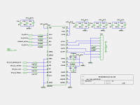
I'm glad you like the idea. I believe it was right to place the dividers in the digital domain. If you X-ray an AB-1.2 you'll see that the routing around the dividers also split the ground plane.
I have attached a schematic of the way I use dividers in my CD player. (The other two pages are just boring special connectors, so I omitted them.)
It uses the SiLabs SI8641EC-B-IS1 is nice because it defaults to '1' (i.e. UART TX or SPI CSN are not activated.) It fits in a narrow SOIC16, and the price isn't off the planet. Other than that I have no reason to choose Si's technology over any other isolator.
This board plays music and seems to work very well. MCLK is passed to the module, and I2S is passed from it through Iso3. Iso1 isn't 100% done yet. In this prototype it transfers the MCLK selector to the clock in the analog domain). For the future I might add UART for HID commands and ignore Resete/Prog.
The RC filters which work in paralell with S1 is something I'm not using. It was a way to experiment with the module setting its own Prog and Reset through GPIO pins.
The way I'm using it not the module is Host powered. The optocoupler would add a device-controlled power gate. The isolators would consume power from USB, so I'm using the coupler to save current.
Børge
Attachments
Thanks for the schematics and suggestions!
Now you mention x-ray, it sounds like you are using 4 layer pcb. I was actually planning on using 2 layer with gnd on component side and vdd on solder side (where possible). Not perfect for decoupling but so much cheaper...
Is it worth it to upgrade to 4 layer to get better decoupling and easier routing?
Artists use 2 layers
Highly recommended: http://www.hottconsultants.com/pdf_files/june2001pcd_mixedsignal.pdf
Børge
Highly recommended: http://www.hottconsultants.com/pdf_files/june2001pcd_mixedsignal.pdf
Børge
I was going to post pictures of the boards I just got back from China.
But now I'm scared to knowing there is pro around.
I often point people to Henry Ott's web page.
Cheers,
Don't be shy mate, some may comment and give tips or see things that help you learn
Chris
- Home
- Source & Line
- Digital Source
- Open-source USB interface: Audio Widget