I'd rather put everything but the DAC & power supplies on the board, leaving the option of omitting some parts (such as the clocks) and adding all the required jumpers, connectors, etc. to make it as "flexible" and versatile as it can be.
I'm next to UnixMan.
But will be use this module in the way EVUL likes.
By the way, we can use 5Vusb for all on the usb side.
If you think you can get 100+ people to agree on the same DAC, same IV stage, same power supply configuration (how many separate ones, what for analog & what for digital, ...), same clock circuit, ......, and keep the cost below 50 Euros, then by all means go ahead.
What I proposed is the simplest basic unit that anyone who wants to convert USB to I2S would need, and cannot get unless he pay $150 to buy something ready made. Maybe it is easier just to pay the 150 bucks in the end ......
I want to make my own choice. So count me out for a turn key solution.
best regards,
Patrick
At last this thread is developing fast, very good ")
But lets not get over our selfs, shall we ?
At this point we are just considering all options, no decisions are made, so no purpose of count me in/out game, just constructive discussion.
Eric has visualized for us what really can be called "ultimate" I2S source, if done right. As previous GB perfectly showed, such product (basically just the uC part) is almost impossible to acquire. Manufacturers are willing to sell whole product, and get their $. That is understandable, we all live by the market rules, so placing us in position of users. This is opportunity to stop being only users and buy overpriced products. So again, for this purpose we only need to buy developed (and preferably preprogrammed) uC with software (drivers), or if it is possible (in means of willingness and brain power), develop it here. This is the hardest part as I see it. More research is needed for choosing "most attractive" uC platform, in terms of pricing/licensing/programing attractiveness. We desperately need comments from experienced embedded programmers, that potentiality could contribute to software development.
For reaching some kinda consensus on global design, I personally don't see what this fuss is all about. If Erics block scheme goes to pcb, it's already way ahead of all currently commercially available products for USB to I2S (spdif) that I'm aware of. Closest match would be some pro DAC's in 4 zeros USD zone. So IMO it is perfect choice for those who want to buy&forget this hard part of PC->I2S section. If others feel like they want to realize their ideas or experiment or feel DIY'ing fun or whatever, they should have opportunity to only buy uC and software, or Uc + software + bare PCB (option for placing clocks on "dirty" side should be provided).
EUVL idea of dividing this PCB to separate modules is very good and worth considering IMHO. This concept would have all the advantages that Eric has already named. Biggest drawback I think would be increased overall price for buy&forget people and maybe somehow decreased performance (it is integral part of modulus design).
You can get a Ayre QB-9 (new) for USD2500. That is really buy and forget.
As one can tell, USB audio is hot, and everyone who has a firmware solution for a uP which otherwise costs <10USD makes 100+ bucks from a "reference solution" which is essentially programmed chip plus a few other components. Let's see what xmos whats for licensed fees per chip.
I am not against buying pre-programmed chips. It depends on how much they cost.
Patrick

Ouch... 11500Eu minimum for Thesycon drivers
So only Centrance pricing left to investigate, or it's automatic no-go for xmos solution ?
Windows drivers development is really large and man hour consuming job, so this pricing is somehow ok. for planed 1000+ products release, but in our case it's makes no sense.
Has anyone heard something about microsoft plans for native windows usbaudio.sys 2.0 driver support ?
Just go ahead and get a KNJN (fpga4fun.com) cheap Altera Cyclone/FX2 USB card (Saxo / Xylo, or some other vendor, or DIY the whole thing after some kind of proof of concept work with some FPGA kit) and implement the ASIO driver yourself. No need to pay thousands for drivers.
Actually here's your proof of concept (Xilink + FX2):
USB Audio - Rigisystems
It can be done by anyone.
"Reference boards production including license (m.o.q. 10u) per unit US$ 204" (group buy anyone?)
USB Audio - Rigisystems
It can be done by anyone.
"Reference boards production including license (m.o.q. 10u) per unit US$ 204" (group buy anyone?)
Last edited:
Hi Patrick,
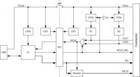
no-no, there must be a misunderstanding here. This isn't at all what I was proposing to do. And (as far as I have understood), neither it is what Eric Juaneda meant. If I'm not wrong, on his diagram the DAC block was included only to show and clarify the whole picture, not to mean that it is part of the project. 
AFAICT nobody proposed to design a complete, finished DAC with async USB input here. Surely PSUs, DAC, I/V, etc. should be left to anyone's own choices. I want to be free to try and choose whatever I like as much as you do.
What I had (and have) in mind is something not very different from what you propose. That is, only USB to I2S, nothing else. But I want it "done right"!
That is, in the best possible way. Which IMHO necessarily implies (among the other things) a clean clock and properly clocked signals on the DAC side and the best possible isolation from the computer / USB bus noise, grounds, etc. Hence something like what's depicted in Eric's block diagram.
IMHO there may be various useful options on this "thing".
One is about the clock(s). That is, whether to mount them on the USB to I2S board, on (your own) DAC board or on a separate, dedicated clock board.
Either way a clean, low jitter clock will be on the "clean" side and is (or can be) directly connected to the DAC as it should.
In principle, it doesn't matter where the clocks are mounted. The overall design and its functioning remains exactly the same. The only concern is about the transmission of the clock signal and the jitter increase that this may cause (I'd say not much if done properly, but surely quite a bit if done badly).
Mounting the clocks (+ clock "switch") on the USB->I2S board or on a board on their own IMHO should not make any difference (does it?). But having them on a separate board will surely cost more money, so why bother?
I'm sure many people will like to use whatever DAC they like (perhaps the one they already have...) without messing too much with it. Having the proper clock generated (and selected) on the USB->I2S board, one may have different options to do that. Even with little or no modification at all to the existing DAC.
Of course someone else will rather prefer to have the clock as close as possible to the DAC chip instead. Doing that will almost surely require a custom DAC board (or some more in-depth mods to an existing one), as you need to provide a way to control (select) the appropriate clock according to the control line coming from the USB->I2S board as well as sending the selected clock signal back to it.
Nonetheless, the same USB->I2S board can be used. All that is required is to omit to mount the clocks and clock "switch" on the USB->I2S board and feed in the (proper) clock signal back from the DAC board.
Of course, proper connections for both modes of operation (clock in & out, clock control line out) should be provided on the SB->I2S board.
(should we like to do so, it may even be possible to provide some quick, easy way to disable the internal clocks and enable the external one using jumpers or dip-switches. That way a fully stuffed board may be used in both ways without modifications).
Another option that I can imagine is about avoiding isolation, reclocking, etc. That is exactly with what you proposed: just the uC, a few required supporting components and a bunch of connectors.
But this can be done also with the same board implementing Eric's design: all that is required is to provide the option of not installing (and easily by-passing) isolators and related circuitry and/or providing some extra connectors on the board.
Yet the user will still have the choice as to whether place the clocks on board or provide it externally.
This is what I meant with "flexibility"... basically one board fits all needs.
Uh?If you think you can get 100+ people to agree on the same DAC, same IV stage, same power supply configuration (how many separate ones, what for analog & what for digital, ...), same clock circuit, ......,
no-no, there must be a misunderstanding here. This isn't at all what I was proposing to do. And (as far as I have understood), neither it is what Eric Juaneda meant. If I'm not wrong, on his diagram the DAC block was included only to show and clarify the whole picture, not to mean that it is part of the project. AFAICT nobody proposed to design a complete, finished DAC with async USB input here. Surely PSUs, DAC, I/V, etc. should be left to anyone's own choices. I want to be free to try and choose whatever I like as much as you do.
What I had (and have) in mind is something not very different from what you propose. That is, only USB to I2S, nothing else. But I want it "done right"!
That is, in the best possible way. Which IMHO necessarily implies (among the other things) a clean clock and properly clocked signals on the DAC side and the best possible isolation from the computer / USB bus noise, grounds, etc. Hence something like what's depicted in Eric's block diagram.
IMHO there may be various useful options on this "thing".
One is about the clock(s). That is, whether to mount them on the USB to I2S board, on (your own) DAC board or on a separate, dedicated clock board.
Either way a clean, low jitter clock will be on the "clean" side and is (or can be) directly connected to the DAC as it should.
In principle, it doesn't matter where the clocks are mounted. The overall design and its functioning remains exactly the same. The only concern is about the transmission of the clock signal and the jitter increase that this may cause (I'd say not much if done properly, but surely quite a bit if done badly).
Mounting the clocks (+ clock "switch") on the USB->I2S board or on a board on their own IMHO should not make any difference (does it?). But having them on a separate board will surely cost more money, so why bother?
I'm sure many people will like to use whatever DAC they like (perhaps the one they already have...) without messing too much with it. Having the proper clock generated (and selected) on the USB->I2S board, one may have different options to do that. Even with little or no modification at all to the existing DAC.
Of course someone else will rather prefer to have the clock as close as possible to the DAC chip instead. Doing that will almost surely require a custom DAC board (or some more in-depth mods to an existing one), as you need to provide a way to control (select) the appropriate clock according to the control line coming from the USB->I2S board as well as sending the selected clock signal back to it.
Nonetheless, the same USB->I2S board can be used. All that is required is to omit to mount the clocks and clock "switch" on the USB->I2S board and feed in the (proper) clock signal back from the DAC board.
Of course, proper connections for both modes of operation (clock in & out, clock control line out) should be provided on the SB->I2S board.
(should we like to do so, it may even be possible to provide some quick, easy way to disable the internal clocks and enable the external one using jumpers or dip-switches. That way a fully stuffed board may be used in both ways without modifications).
Another option that I can imagine is about avoiding isolation, reclocking, etc. That is exactly with what you proposed: just the uC, a few required supporting components and a bunch of connectors.
But this can be done also with the same board implementing Eric's design: all that is required is to provide the option of not installing (and easily by-passing) isolators and related circuitry and/or providing some extra connectors on the board.
Yet the user will still have the choice as to whether place the clocks on board or provide it externally.
This is what I meant with "flexibility"... basically one board fits all needs.
that's crazy. No go.received now the doc. about Windows drivers for Xmos with price
Question is: do we need their custom driver dev kit? Isn't there a ready-made (non-demo!) "generic" windows driver from Xmos?
BTW, personally I only care about Linux drivers.
Last edited:
If you look at Ayre QB9, or papers from Hawksford, or indeed comments from Jocko and the like, you want to place the clock at the DAC, not the uP.
That can only mean outside the module we are discussing here, as everyone has his own DAC choice.
And if you want to do the clock right (lowest jitter), there is only one choice IMHO -- differential Colpitts driving ECL logic.
http://www.diyaudio.com/forums/digital-source/154401-differential-clock-4.html#post2054656
Not everyone want this complexity.
Buying a Crystek XO and adding a LT1761 is for me not lowest jitter.
Hence my proposal.
But till now there is no chip which comes with affordable software, so we might well be discussing for nothing....
Patrick
Patrick
For your interest :
Multi Channel I2S Output
Koon said on the page, "My final aim is to play LINN Studio Master format." which is 24/192 ??
Wonder if he has already achieved that.
Patrick
PS already PM him for the question.
Multi Channel I2S Output
Koon said on the page, "My final aim is to play LINN Studio Master format." which is 24/192 ??
Wonder if he has already achieved that.
Patrick
PS already PM him for the question.
that's crazy. No go.
Question is: do we need their custom driver dev kit? Isn't there a ready-made (non-demo!) "generic" windows driver from Xmos?
BTW, personally I only care about Linux drivers.
No windows driver is provided with xmos reference design as I understand (please correct me if I'm wrong), so I raise a question regarding native windows USB2.0 audio support (lucky MAC users have it).
Without windows support, no chance of getting same amount of buyers on board, it's clear i think.
Thank you mhelin for your ideas and link

Regarding "DIY the whole thing after some kind of proof of concept work with some FPGA kit" part, personally my programing skills ended up in 90's with PIC family and ASM
Still no high level language programmers for volunteering showed up.Maybe we should really concentrate on uC and software part and leave other aspects behind for now, because without it, we are only left with commercial products and limited customizing options.
Currently looking through fpga4fun.com and other links, looks very promising !
what do you mean? physically or logically?If you look at Ayre QB9, or papers from Hawksford, or indeed comments from Jocko and the like, you want to place the clock at the DAC, not the uP.
From a logical point of view, with Eric's diagram the clock is "at the DAC" (and is sent back to the uC from there).
From a "physical" point of view, if you mount the clocks on the uC board of course it will not be "at" the DAC (yet likely only a few cm apart).
But does this really matters? or is it more a matter of proper connections (impedance matched lines) and terminations?
sure, that's exactly my point!Not everyone want this complexity.
If you want to make it simple, install the clocks on the uC board.
If you want to go fancy, just leave that part of the board empty. Place whatever "super" clock(s) next to your DAC and feed it back to the uC board.
That's it.
As said, the board should support both clock input(s) & output(s) as well as a "clock switch" control line (which tells you the SR "family" of the incoming stream) to make your design as simple as possible even if you decide to go fancy. With a diagram like Eric's one, that's easy to do. Basically it's just a matter of adding the required connectors.
indeed. That's sad...But till now there is no chip which comes with affordable software, so we might well be discussing for nothing....
Originally Posted by EUVL
But till now there is no chip which comes with affordable software, so we might well be discussing for nothing....
nah some fpga thing would work in that case, what peufeu 's crew wanted to do before vanishing. They supposed to have something.
I dont care if my r2r dac is further away from the uC&clock (maybe even 4-5 meters away with LVDS , which I plan to do) , I just use an r2r dac anyway
 .
.Oh and many ppl intend to use this thing with ASRC dac. Ha!
Last edited:
- Status
- This old topic is closed. If you want to reopen this topic, contact a moderator using the "Report Post" button.
- Home
- Source & Line
- Digital Source
- Ultimate USB to I2S interface