This is hived off from a thread about M2Tech HiFace 24/192 USB transport.
I have noticed a slight sharp edge to the sound of my modded HiFace set-up when using I2S as compared to SPDIF.
My I2S lines a short (1") & I'll work on improving them but I've been thinking that one explanation for this might be the SPDIF transformer providing galvanic isolation from the DAC. So I'm back to this old chestnut again of galvanic isolation.
Here's my summary of the info posted on this in that thread so far:
- high-speed USB 2.0(480Mbps) cannot be so isolated with currently available technology.
- isolating I2S will introduce jitter (using ADUM, etc)
- this could be an acceptable trade-off - Jitter Vs ground Noise
- if MCLK is rec-clocked after the I2S isolation it might be more acceptable.
One further thought occurred to me - what about splitting the I2S signal & going differential to two DACs i.e one DAC process R+/- & the other processing L+/-.
Would this achieve the same result as galvanic isolation in that it would remove common noise? I don't suppose the simpler version of one DAC processing R+/L+ & the other processing R-/L- would remove common noise (as effectively or at all?).
Can it be done effectively at 24/192 speeds?
Has anybody got any experience in using i2S balanced?
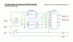
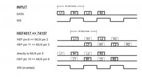
There is a Pedja Rogic PDF attached which shows how to split I2S for R+/- & L+/- use but it uses a discontinued chip (4517) & it is directed towards 16/44 operation
I have noticed a slight sharp edge to the sound of my modded HiFace set-up when using I2S as compared to SPDIF.
My I2S lines a short (1") & I'll work on improving them but I've been thinking that one explanation for this might be the SPDIF transformer providing galvanic isolation from the DAC. So I'm back to this old chestnut again of galvanic isolation.
Here's my summary of the info posted on this in that thread so far:
- high-speed USB 2.0(480Mbps) cannot be so isolated with currently available technology.
- isolating I2S will introduce jitter (using ADUM, etc)
- this could be an acceptable trade-off - Jitter Vs ground Noise
- if MCLK is rec-clocked after the I2S isolation it might be more acceptable.
One further thought occurred to me - what about splitting the I2S signal & going differential to two DACs i.e one DAC process R+/- & the other processing L+/-.
Would this achieve the same result as galvanic isolation in that it would remove common noise? I don't suppose the simpler version of one DAC processing R+/L+ & the other processing R-/L- would remove common noise (as effectively or at all?).
Can it be done effectively at 24/192 speeds?
Has anybody got any experience in using i2S balanced?
There is a Pedja Rogic PDF attached which shows how to split I2S for R+/- & L+/- use but it uses a discontinued chip (4517) & it is directed towards 16/44 operation
Attachments
Hello Jkeny,
I've also encountered this problem regarding transporting I2S signals but now I find a trade-off sollution which (from theory) it must work: try transporting I2S using LVDS. I've choosed few chips maded by TI but any other LVDS manufacturer should provide good parts (like National Semiconductors, Fairchild, On Semiconductors, etc).
The chip I've choosed to receive/"decode" LVDS signals is SN65LVDS2 in SOT23-5 (not mandatory") . Of course, I could choose a chip with 4 receivers on the same die but in my mind I thought that it could be better to have a separate PSU track for every LVDS receiver.
. Of course, I could choose a chip with 4 receivers on the same die but in my mind I thought that it could be better to have a separate PSU track for every LVDS receiver.
I hope it help you,
L
I've also encountered this problem regarding transporting I2S signals but now I find a trade-off sollution which (from theory) it must work: try transporting I2S using LVDS. I've choosed few chips maded by TI but any other LVDS manufacturer should provide good parts (like National Semiconductors, Fairchild, On Semiconductors, etc).
The chip I've choosed to receive/"decode" LVDS signals is SN65LVDS2 in SOT23-5 (not mandatory
. Of course, I could choose a chip with 4 receivers on the same die but in my mind I thought that it could be better to have a separate PSU track for every LVDS receiver.I hope it help you,
L
I was looking to go with balanced I2S anyway, so I'm wondering would differential line drivers/receivers do the job DS8921/22 for instance. Would these be fast enough, low jitter? I know ECDesigns has used them in his I2S synchronous re-clocker but this was for 16/44 - I'm looking at 24/192 signals.
Can it be done effectively at 24/192 speeds?
Has anybody got any experience in using i2S balanced?
There is a Pedja Rogic PDF attached which shows how to split I2S for R+/- & L+/- use but it uses a discontinued chip (4517) & it is directed towards 16/44 operation
Thanks for sharing that schematic, its helping me with a design I'm currently thinking about
The HEF4517 is still in full production according to NXP, however from the datasheet that circuit isn't guaranteed to work, though typically it will. It could never be made to work at 192kHz since that requires a bit clock frequency over 10MHz. Increasing the supply to the 4517 to 15V might do the trick though, then level shifters will be needed...
In any case I don't at the moment see how this circuit might take the place of galvanic isolation. If you've got ground currents, once they've been translated into noise at the bit-clock receiver, there's no way to undo the damage. That's because the generated error from the jitter is data-related - a jitter error when you've got digital silence is a different matter from a jitter error at full scale.
I'm currently investigating isolation schemes for my own project so will post something when I've got it to offer... As a first attempt, I think jitter only matters on the bit clock, not the other signals. So we only need to pay attention to that signal - others can have major jitter without any audible effects.
Low jitter clock receivers
Those parts look to have been designed for the old-style hard disks - I'm just about old enough to remember ST506 interfaces
Although they're fast enough, I'd not use them as their skew figures give some indication of the inherent jitter - worst case 2.75nS for the A variant. They're over-specified on common mode input voltage range, being usable on RS422 lines.
LVDS solutions I think would be a better choice. Have a look at DS90LV028AQ (receiver) and DS90LV027AQ (transmitter) instead.
I was looking to go with balanced I2S anyway, so I'm wondering would differential line drivers/receivers do the job DS8921/22 for instance. Would these be fast enough, low jitter? I know ECDesigns has used them in his I2S synchronous re-clocker but this was for 16/44 - I'm looking at 24/192 signals.
Those parts look to have been designed for the old-style hard disks - I'm just about old enough to remember ST506 interfaces
Although they're fast enough, I'd not use them as their skew figures give some indication of the inherent jitter - worst case 2.75nS for the A variant. They're over-specified on common mode input voltage range, being usable on RS422 lines.
LVDS solutions I think would be a better choice. Have a look at DS90LV028AQ (receiver) and DS90LV027AQ (transmitter) instead.
LVDS is a better spec but I also wanted to try achieve a R+/- & L+/- I2S signal stream as I'm thinking of using two DACs for balanced operation. It seems crazy to go SE to BAL & BAL back to SE for the LVDS process & then have to convert SE to BAL again! Any ideas?Those parts look to have been designed for the old-style hard disks - I'm just about old enough to remember ST506 interfaces
Although they're fast enough, I'd not use them as their skew figures give some indication of the inherent jitter - worst case 2.75nS for the A variant. They're over-specified on common mode input voltage range, being usable on RS422 lines.
LVDS solutions I think would be a better choice. Have a look at DS90LV028AQ (receiver) and DS90LV027AQ (transmitter) instead.
I have noticed a slight sharp edge to the sound of my modded HiFace set-up when using I2S as compared to SPDIF.
I would rather test the premiss that the "slight sharp edge " is indeed due to ground noise before jumping off the deep end of USB/I2S isolation. Not that it isn't worhtwhile. Only the cure may end up being worse than the ailment.
I would rather test the premiss that the "slight sharp edge " is indeed due to ground noise before jumping off the deep end of USB/I2S isolation. Not that it isn't worhtwhile. Only the cure may end up being worse than the ailment.
I agree, it is a premise, based on the differnce I percieved in sound between SPDIF & I2S into the same Buffalo DAC. I know there are a lot of other parameters & differences that come into play here but I've tried it on a number of other DACs also & the same general difference in sound applies - SPDIF has a silky smooth sound with a good depth to the sound-stage; I2S has a more edgy & forward sound with less depth to the sound-stage.
The question really is - is I2S signal integrity or ground noise the cause of this ? I have a 100MHz scope but lack the competence in using it to verify signal integrity.
I have taken out the original 1" of wiring & replaced it with about 3" of individual twisted pairs for BCK,LRCK & DATA with some separation between them. I haven't connected it back together yet to listen & won't be able to for a while.
I guess one way of teasing out the issue would be to bypass the SPDIF output transformer by using instead a resistive divider for 75ohm impedance on the output of the DIT4192 SPDIF generating chip. This experiment will have to wait a while though.
LVDS is a better spec but I also wanted to try achieve a R+/- & L+/- I2S signal stream as I'm thinking of using two DACs for balanced operation. It seems crazy to go SE to BAL & BAL back to SE for the LVDueS process & then have to convert SE to BAL again! Any ideas?
I'm not really sure from this what you're trying to achieve. Do you mean you want to send normal data from I2S into one DAC, and inverted data into another? If so, that will maybe improve SNR by 3dB and cancel out any 2nd order distortion components in the DACs. Such a differential configuration is easily implemented together with the LVDS balancing - to generate + and - data just choose the receivers without the termination resistors (-A rather than -AQ suffix) and correct them with opposite polarities, remembering to add an external termination. The step from SE to BAL (or back again) in digital is quite a lot simpler than in analog - just one of those LVDS chips does the trick. Since the DACs don't have BAL inputs, the conversion from BAL to SE is inevitable.
I would rather test the premiss that the "slight sharp edge " is indeed due to ground noise before jumping off the deep end of USB/I2S isolation. Not that it isn't worhtwhile. Only the cure may end up being worse than the ailment.
I'm wondering what full galvanic isolation might achieve, given that the DAC is going straight into headphones in this case- i.e. not into any other equipment with a ground referenced connection. If the DAC was being fed into a preamp, then on to a power amp it may well be justified. Another thing to try which is way, way simpler is to feed the cables between the computer and DAC through a series of ferrites to absorb RF hash wanting to travel out from the USB port. A few of the clip-on kinds of ferrites will certainly clean things up if applied at right next to the USB port.
I'm wondering what full galvanic isolation might achieve
Me too. I also suspect that it's not quite the same whether you isolate USB, I2S or somewhere further downstream. In my own anecdotal experience using a 2707 into an ASRC and a 1794 with a transformer output, there is no audible difference whether the grounds before and after the transformer are connected. Of course there must be lots of capacitive coupling anyway.
I was hoping that getting a differential I2S signal as in the attached pic might also have the added benefit of cancelling common mode noise but I may be wrong?I'm not really sure from this what you're trying to achieve. Do you mean you want to send normal data from I2S into one DAC, and inverted data into another? If so, that will maybe improve SNR by 3dB and cancel out any 2nd order distortion components in the DACs. Such a differential configuration is easily implemented together with the LVDS balancing - to generate + and - data just choose the receivers without the termination resistors (-A rather than -AQ suffix) and correct them with opposite polarities, remembering to add an external termination. The step from SE to BAL (or back again) in digital is quite a lot simpler than in analog - just one of those LVDS chips does the trick. Since the DACs don't have BAL inputs, the conversion from BAL to SE is inevitable.
Attachments
I'm wondering what full galvanic isolation might achieve, given that the DAC is going straight into headphones in this case- i.e. not into any other equipment with a ground referenced connection. If the DAC was being fed into a preamp, then on to a power amp it may well be justified. Another thing to try which is way, way simpler is to feed the cables between the computer and DAC through a series of ferrites to absorb RF hash wanting to travel out from the USB port. A few of the clip-on kinds of ferrites will certainly clean things up if applied at right next to the USB port.
Ah well, the real difference in sound between I2S & SPDIF is only noticeable when using a full preamp/amp rig & not noticeable when using the headphones.
Hmm, I'll experiment with ferrites!
I'm not with you here - I see one I2S stream from the pic above fed to a Vout DAC creating R+ & R- at it's analog outs. And the other DAC would similarly create L+ & L-. These analog signals could be fed to a balanced headphone or balanced preamp/amp............... Since the DACs don't have BAL inputs, the conversion from BAL to SE is inevitable.
I imagine that R+/- being generated in one DAC would have better common mode noise cancellation than if R+/L+ was generated in one DAC & R-/L- in another DAC but it may not be worth the extra effort necessary to achieve this?
Last edited:
Advantage of balanced mains supply
Ah, well now it makes more sense to me. I've just upgraded my rig by fitting mains isolation in the power feed to my active speakers and CD player and DAC. This works a treat - means that there's no route for mains hash to get into the system now. I suggest you try the same - in the power feed to your pre/power combination.
I bought two 230V -> 115V 500VA toroids and wired them up to balance the mains feed. So instead of a live wire with 230VAC and a neutral which is close to earth, I now have two 115V wires 180degrees out of phase. The centre point of the two secondaries is connected to earth. This means firstly that incoming RF on the mains gets shunted to ground. But more importantly, the capacitive coupling across the toroids in my active speakers and DAC is considerably reduced, because now they're receiving a balanced power signal rather than a single-ended one. Whereas before I was getting upto 200uA current out of the signal ground into other equipment, now its around 5uA.
Ah well, the real difference in sound between I2S & SPDIF is only noticeable when using a full preamp/amp rig & not noticeable when using the headphones.
Ah, well now it makes more sense to me.
I've just upgraded my rig by fitting mains isolation in the power feed to my active speakers and CD player and DAC. This works a treat - means that there's no route for mains hash to get into the system now. I suggest you try the same - in the power feed to your pre/power combination.I bought two 230V -> 115V 500VA toroids and wired them up to balance the mains feed. So instead of a live wire with 230VAC and a neutral which is close to earth, I now have two 115V wires 180degrees out of phase. The centre point of the two secondaries is connected to earth. This means firstly that incoming RF on the mains gets shunted to ground. But more importantly, the capacitive coupling across the toroids in my active speakers and DAC is considerably reduced, because now they're receiving a balanced power signal rather than a single-ended one. Whereas before I was getting upto 200uA current out of the signal ground into other equipment, now its around 5uA.
Ground isolation
That's exactly what the LVDS transmitters give you - a differential signal - not just for the data lines, but all of it. It means that ground noise has a much reduced effect. So for example, if you're having trouble in a particular set-up with conducted RF along the ground, you can deal with this with a choke in the ground wire. Or with ferrites over the cable. Using the LVDS means you can now tolerate upto 1V of common mode voltage i.e. upto 1V difference in the ground potentials between transmit and receive sides. Any clearer now?
Full galvanic isolation means you can have potentially a couple of kV difference between two grounds, which looks a bit like overkill in this application where you just want to be rid of some RF!
Yes, you're right. If you want to use more DACs, that's the way to go. But using more DACs is really only useful if the audible noise of a single one is a problem for you, or there's significant 2nd order distortion in their outputs which is common between them. In this case, you'll get common mode cancellation of the audio band noise, but not common mode cancellation up to RF frequencies which is what I thought you wanted. Perhaps that's been the misunderstanding - when we're talking about common-mode cancellation, there's a difference between audio band cancellation and RF cancellation.
I was hoping that getting a differential I2S signal as in the attached pic might also have the added benefit of cancelling common mode noise but I may be wrong?
That's exactly what the LVDS transmitters give you - a differential signal - not just for the data lines, but all of it. It means that ground noise has a much reduced effect. So for example, if you're having trouble in a particular set-up with conducted RF along the ground, you can deal with this with a choke in the ground wire. Or with ferrites over the cable. Using the LVDS means you can now tolerate upto 1V of common mode voltage i.e. upto 1V difference in the ground potentials between transmit and receive sides. Any clearer now?
Full galvanic isolation means you can have potentially a couple of kV difference between two grounds, which looks a bit like overkill in this application where you just want to be rid of some RF!
I imagine that R+/- being generated in one DAC would have better common mode noise cancellation than if R+/L+ was generated in one DAC & R-/L- in another DAC but it may not be worth the extra effort necessary to achieve this?
Yes, you're right. If you want to use more DACs, that's the way to go. But using more DACs is really only useful if the audible noise of a single one is a problem for you, or there's significant 2nd order distortion in their outputs which is common between them. In this case, you'll get common mode cancellation of the audio band noise, but not common mode cancellation up to RF frequencies which is what I thought you wanted. Perhaps that's been the misunderstanding - when we're talking about common-mode cancellation, there's a difference between audio band cancellation and RF cancellation.
Last edited:
But the differential signal coming out of the LVDS transmitter can't be used as a direct feed into a DAC to give balanced feed to the DAC, I presume. It has to go through the LVDS receiver which converts it back to SE & I then have to use some SE to BAL converter to feed the DACs a balanced signal - maybe that is the best way to do it but it seems so roundabout?That's exactly what the LVDS transmitters give you - a differential signal - not just for the data lines, but all of it. It means that ground noise has a much reduced effect. So for example, if you're having trouble in a particular set-up with conducted RF along the ground, you can deal with this with a choke in the ground wire. Or with ferrites over the cable. Using the LVDS means you can now tolerate upto 1V of common mode voltage i.e. upto 1V difference in the ground potentials between transmit and receive sides. Any clearer now?
Well, yes I wanted CM noise cancellation at all frequencies. Would using a DAC operating from a differential signal not cancel all the common noise, not just in the audio band?Full galvanic isolation means you can have potentially a couple of kV difference between two grounds, which looks a bit like overkill in this application where you just want to be rid of some RF!
Yes, you're right. If you want to use more DACs, that's the way to go. But using more DACs is really only useful if the audible noise of a single one is a problem for you, or there's significant 2nd order distortion in their outputs which is common between them. In this case, you'll get common mode cancellation of the audio band noise, but not common mode cancellation up to RF frequencies which is what I thought you wanted. Perhaps that's been the misunderstanding - when we're talking about common-mode cancellation, there's a difference between audio band cancellation and RF cancellation.
I wanted to go differential into 2 DACs anyway & thought it might also be a way of cancelling any ground noise riding on the signal line - that's all really.
So, I'm looking for the easiest, smartest way of achieving this & I posed this as a question
Last edited:
Sorry, Abraxalito, I missed this post & I see that in it, you've answered all my subsequent questions, so sorry for repeating them & appearing dumbThanks for sharing that schematic, its helping me with a design I'm currently thinking about
The HEF4517 is still in full production according to NXP, however from the datasheet that circuit isn't guaranteed to work, though typically it will. It could never be made to work at 192kHz since that requires a bit clock frequency over 10MHz. Increasing the supply to the 4517 to 15V might do the trick though, then level shifters will be needed...
In any case I don't at the moment see how this circuit might take the place of galvanic isolation. If you've got ground currents, once they've been translated into noise at the bit-clock receiver, there's no way to undo the damage. That's because the generated error from the jitter is data-related - a jitter error when you've got digital silence is a different matter from a jitter error at full scale.
I'm currently investigating isolation schemes for my own project so will post something when I've got it to offer... As a first attempt, I think jitter only matters on the bit clock, not the other signals. So we only need to pay attention to that signal - others can have major jitter without any audible effects.
I see what you're saying about ground currents being converted to noise on the bit clock - I guess I was treating the DAC like an op-amp, doh!
I'm interested in hearing about your results with BCK isoaltion
Dealing with CM noise
I'm wondering if my terminology isn't precise enough here, so I'm gonna make an attempt to clarify a bit more... By 'DAC' I'm talking about the chip that does the job (like TDA1545 for example), not the whole unit. So yes, given that no DAC chips I've seen have differential inputs, you'd need an LVDS receiver between the differential I2S and the chip. So no, I can't see the need here for 'some SE to BAL converter'. The two (+ and -) DAC chips can be fed from the same differential I2S data line via LVDS receivers connected in opposite polarity.
I think I might have been less than clear on this point too. The rejection of CM noise is a function of the receiver, not the transmitter. So when you're feeding headphones, the fact they have no ground connection means they're very good at rejecting CM noise, at all frequencies. But I guess your preamp has a SE input, and that's the problem here. Even running + and - DACs will need a Bal-SE conversion stage before going out to the preamp. Then the CM noise is picked up by the preamp, so all advantage (in CM noise) of running balanced is lost. So to deal with CM noise effectively, we need a systems-wide solution, it can't be fixed just in the DAC unit. Make better sense now?
Yep, it is, provided the next element in the chain has a balanced input with good CM rejection.
But the differential signal coming out of the LVDS transmitter can't be used as a direct feed into a DAC to give balanced feed to the DAC, I presume. It has to go through the LVDS receiver which converts it back to SE & I then have to use some SE to BAL converter to feed the DACs a balanced signal - maybe that is the best way to do it but it seems so roundabout?
I'm wondering if my terminology isn't precise enough here, so I'm gonna make an attempt to clarify a bit more... By 'DAC' I'm talking about the chip that does the job (like TDA1545 for example), not the whole unit. So yes, given that no DAC chips I've seen have differential inputs, you'd need an LVDS receiver between the differential I2S and the chip. So no, I can't see the need here for 'some SE to BAL converter'. The two (+ and -) DAC chips can be fed from the same differential I2S data line via LVDS receivers connected in opposite polarity.
Well, yes I wanted CM noise cancellation at all frequencies. Would using a DAC operating from a differential signal not cancel all the common noise, not just in the audio band?
I think I might have been less than clear on this point too. The rejection of CM noise is a function of the receiver, not the transmitter. So when you're feeding headphones, the fact they have no ground connection means they're very good at rejecting CM noise, at all frequencies. But I guess your preamp has a SE input, and that's the problem here. Even running + and - DACs will need a Bal-SE conversion stage before going out to the preamp. Then the CM noise is picked up by the preamp, so all advantage (in CM noise) of running balanced is lost. So to deal with CM noise effectively, we need a systems-wide solution, it can't be fixed just in the DAC unit. Make better sense now?
I wanted to go differential into 2 DACs anyway & thought it might also be a way of cancelling any ground noise riding on the signal line - that's all really.
Yep, it is, provided the next element in the chain has a balanced input with good CM rejection.
Sorry, yes, I'm being really dumb here - I'm having a brain haze mixing up how balanced analog works using two lines carrying R+/- & two lines carrying L+/- with how balanced digital would work using one line for R+/L+ & one line for R-/L-.I'm wondering if my terminology isn't precise enough here, so I'm gonna make an attempt to clarify a bit more... By 'DAC' I'm talking about the chip that does the job (like TDA1545 for example), not the whole unit. So yes, given that no DAC chips I've seen have differential inputs, you'd need an LVDS receiver between the differential I2S and the chip. So no, I can't see the need here for 'some SE to BAL converter'. The two (+ and -) DAC chips can be fed from the same differential I2S data line via LVDS receivers connected in opposite polarity.
Yes, I intend to use balanced all the way to the speakers!I think I might have been less than clear on this point too. The rejection of CM noise is a function of the receiver, not the transmitter. So when you're feeding headphones, the fact they have no ground connection means they're very good at rejecting CM noise, at all frequencies. But I guess your preamp has a SE input, and that's the problem here. Even running + and - DACs will need a Bal-SE conversion stage before going out to the preamp. Then the CM noise is picked up by the preamp, so all advantage (in CM noise) of running balanced is lost. So to deal with CM noise effectively, we need a systems-wide solution, it can't be fixed just in the DAC unit. Make better sense now?
Yep, it is, provided the next element in the chain has a balanced input with good CM rejection.
- Status
- This old topic is closed. If you want to reopen this topic, contact a moderator using the "Report Post" button.
- Home
- Source & Line
- Digital Source
- I2S ground noise issues & possible resolutions