

Re: ZIP Flie
Hi
I digged up AN DAC kit 1.1 circuit but it is 700k (cannot be attached)
Mail me offline if you want a copy
Info@TENTlabs.com
regards
Audiofanatic said:Hi guys,
Please give Jesús a break.
Here is the ZIP File.
Audiofanatic
BTW the moderator knows about this!
Hi
I digged up AN DAC kit 1.1 circuit but it is 700k (cannot be attached)
Mail me offline if you want a copy
Info@TENTlabs.com
regards
And for anybody interested in other DACs, here's a link to 3rd Kusunoki DAC http://www.diyaudio.com/forums/showthread.php?s=&postid=173347#post173347
audioPT said:3... sorry for the quality
If you want, send me your mail account as I can send the original.
BTW, I olny send when I have enough mails...
fast job !! (sent Pedro the original file 10 mins ago
Guido
hello PT,
Please send me a copy of the power supply and voltage regulator
Much thanks ,
Sigurd
sigurd21@gmail.com
Please send me a copy of the power supply and voltage regulator
Much thanks ,
Sigurd
sigurd21@gmail.com
Is your interest in repairing a unit, or are you simply curious as to how AN DAC's function?
Is your interest in repairing a unit, or are you simply curious as to how AN DAC's function?
Hi Ken,
actually I'm going to study all the aspects of DAC, my goal is to build my cd player based on AD1865, but listening to speak very well about Audionote DAC I'm curious to give a look to the schematics. Sorry for my English.
Thanks
Bruno
While I don't have AN DAC schematics, I feel rather certain that they are relatively simple. The digital section appears common to all their DACs. It consists of an single RCA input to a AN S/PDIF interface transformer feeding a Cirrus CS8414/CS8416 digital input receiver. After clock and data recovery is performed by the Cirrus chip they are input to an AD1865 DAC chip, as you know. Famously, there is no digital interpolation filter utilized. Even the inter-channel delay, due to the the multiplexed nature of the serial data stream, is left uncorrected, resulting in an (IMHO, inconsequential) 11uS. arrival time difference. The AD1865 current outputs then are passively converted to voltage via AN tantalum resistors. No special steps appear to have been employed to reject incoming clock jitter beyond that provided by the Cirrus DIR chip. That's basically it.
Things get more interesting on the analog side, and vary among the AN line. All utilize vacuum tubes, but the lower range units typically feature capacitor coupled outputs while the upper range units typically feature step-up transformer interfacing within the I/V circuit in addition to single ended transformer coupled outputs. In my estimation/guess, the sound quality AN achieves in their DACs is primarily due to the use of R-2R DAC chip, no digital filter (NOS operation), tube analog stage, and particular passive component selection (i.e., tantalum resistors, black gate electrolytic capacitors, and large mu-metal slit-core single-ended transformers.
Things get more interesting on the analog side, and vary among the AN line. All utilize vacuum tubes, but the lower range units typically feature capacitor coupled outputs while the upper range units typically feature step-up transformer interfacing within the I/V circuit in addition to single ended transformer coupled outputs. In my estimation/guess, the sound quality AN achieves in their DACs is primarily due to the use of R-2R DAC chip, no digital filter (NOS operation), tube analog stage, and particular passive component selection (i.e., tantalum resistors, black gate electrolytic capacitors, and large mu-metal slit-core single-ended transformers.
Last edited:
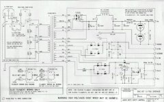
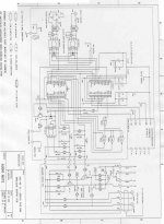
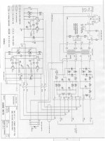
Hi, audioPTHere it go!
in 3 parts...
Counld i have an original copy of your audio note dac kit 1.1 circuit?
If it is ok, my email address is feiwei.nupt@gmail.com
Thank you and best wishes!
- Home
- Source & Line
- Digital Source
- Audio Note DAC Schematic