Bunpei,
I have recently ordered the SDTrans and full SyncDAC set and am awaiting its arrival.
This has me thinking about power supplies.
Will you kindly share more details of the solar cell power supply?
In particular I would like to know more details regarding:
The modification of the panel to reduce the output to 10V
The krypton bulb arrangement
The shunt regulator
Best regards
Jeff
I appreciated your interest in a solar panel based power supply.
In this reply, I answer to some parts of your questions. In the next reply, I will provide additional pictures.
1. How to get 10V output
A solar cell panel I used was originally designed to output about 20 V. The whole unit consists two columns of small cell group connected in series. I cut a cross bar conductor between the columns and separated one unit into two units and connected them in parallel.
(In the next post, I will show you a photo.)
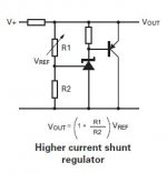
2. Shunt regulator
A basic schematic of the regulator is attached below. A well-experienced DIY builder would use more sophisticated Salas type discrete regulators.
In this reply, I answer to some parts of your questions. In the next reply, I will provide additional pictures.
1. How to get 10V output
A solar cell panel I used was originally designed to output about 20 V. The whole unit consists two columns of small cell group connected in series. I cut a cross bar conductor between the columns and separated one unit into two units and connected them in parallel.
(In the next post, I will show you a photo.)
2. Shunt regulator
A basic schematic of the regulator is attached below. A well-experienced DIY builder would use more sophisticated Salas type discrete regulators.
Attachments
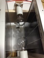
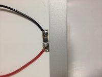
The first picture shows a mechanical structures for bulbs and panels. Wood frames are suitable for making such a structure.
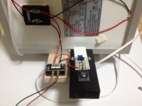
The second pictures shows a small assembly of shunt regulator board.
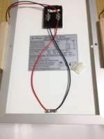
The third picture shows wiring on a panel. In the bottom, a cross bar conductor connection between two columns of solar cell groups is cut and wires are soldered on the cut points.
(The fourth picture shows a close-up of the part.)
I scraped a plastic sheet of the backside of the panel and cut the conductor plate in the middle.
In the case of the panel assembly shown in these photos, four columns of cell groups, each outputs approximately DC +10V, are connected in parallel. Approximately 400mA in total output is available.
This build is fully based on an original design by Mr. Ishida in Tokyo.
The second pictures shows a small assembly of shunt regulator board.
The third picture shows wiring on a panel. In the bottom, a cross bar conductor connection between two columns of solar cell groups is cut and wires are soldered on the cut points.
(The fourth picture shows a close-up of the part.)
I scraped a plastic sheet of the backside of the panel and cut the conductor plate in the middle.
In the case of the panel assembly shown in these photos, four columns of cell groups, each outputs approximately DC +10V, are connected in parallel. Approximately 400mA in total output is available.
This build is fully based on an original design by Mr. Ishida in Tokyo.
Attachments
Last edited:
Some of you may not believe this claim.
However, I'd like to recommend SDTrans users apply such tiny bead cores on a DC +5V power supply line of SDTrans.
The product is originally a "surge absorber" that removes "spikes" in a line. A Japanese friend of mine told me that it was also very effective for improving a total SQ of SDTrans. First, I thought it must be exaggerated somehow. After trying it with my SDTrans actually, I realized its effectiveness.
In the yellow circles marked on the pictures, you find the bead cores.
You can read an explanation of the product here;
Surge Absorbers : Amorophous Products : Hitachi Metals America
An externally hosted image should be here but it was not working when we last tested it.
The key of the bead core is "nanocrystalline material".
Domestic list price of the bead core "Black Pearl" is 600 JPY (= 6 USD) /each. I think it is worth trying really.
If you are interested in the product, please contact to Mr. Teramoto of the following e-mail address;
iphone0123 < at > goo < dot > jp
Hello Bunpei
Have you the contact of Mr. Teramoto ,as you can see the address is not visible.
Thanks.

Hi Bunpei,
I have in my hands the SyncDAC. I did not purchase the I/V PCB from Tachyon because I have transformers that I can use.
I can see an example of how transformers can be connected to the PCB's here:
http://www.diyaudio.com/forums/digi...emory-card-transport-project.html#post3268357
I cannot make out the exact pin connections.
Is it possible for you to clarify using the SyncDAC connections for use with I/V other than Chiaki's I/V?
Kind regards,
Jeff
Hi, Jeff!
It's very nice to hear from an owner of Chiaki's DAC board.
Here are markings, CN13, CN14, CN2 and CN3 for 4-pin headers.
Let's assign pin #1 as the nearest pin located to those CN markings.
Pin #1, Pin #4 ___ GND
Pin #2 ___ in-phase of balanced output
Pin #3 ___ out-of-phase of balanced output
Is this explanation clear enough for you?
Hi Bunpei,
Thank you for your reply.
Both CN2 and CN3 headers are outputs for L Ch
Both CN13 and CN14 headers are outputs for R Ch
From the photo I linked in my last message, it appears the two outputs for each channel are paralleled before feeding into the transformer.
Is this correct?
Kind regards
Jeff
Thank you for your reply.
Both CN2 and CN3 headers are outputs for L Ch
Both CN13 and CN14 headers are outputs for R Ch
From the photo I linked in my last message, it appears the two outputs for each channel are paralleled before feeding into the transformer.
Is this correct?
Kind regards
Jeff
Yes, your guess is correct.
CN2, CN3, CN13 or CN14 is a merged output of 4 DACs at one side of ES9018.
As far as you use your transformer I/V, I think it's better for you to tie
CN2 & CN3 and CN13 and CN14 to obtain more power.
When you use an OpAmp-based I/V module, an output given by 8 DACs in parallel might bring too much current.
Member
Joined 2006
Hi, michyy!
Mr. Yamazaki of Tachyon has a plan for releasing the next batch of Chiaki's DAC.
Please send your estimate request to him.
jack < at > mtc < dot > biglobe < dot > ne < dot > jp
Bunpei
Hi Bunpei san,
Will there be a next batch? Looking forward to it!!
Member
Joined 2006
Hi Bunpei san,
Will there be a next batch? Looking forward to it!!
Oh...just found out from Yamazaki san's website that all from the fourth batch have been sold out at end of May...
But the good news is.....there will be a next lot!…. Just sent him an email to place an order for one.
")
Last edited:
- Home
- Source & Line
- Digital Source
- MicroSD Memory Card Transport Project