I have a problem with a voltage spike being generated on the output on power off. The magnitude is over 1 volt and this is problematic because I have power amplifiers (separate boxes) with high gain after the PGA.
Some basic info
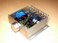
8ch preamp / attenuator
4 * PGA2311
2 * LME49740 input buffer
PIC16F88
Separate supplies for analog and digital (LM317 & LM337) ie three bridges and transformer secondaries
Detailed description of the problem
The transient seems to be generated because -5VA goes down much faster than +5VA. -5VA goes down very quickly as if there was a very low impedance path to ground at power down.
In CS3310 (older and pretty much identical IC in function) datasheet it is advised that analog supplies be applied before digital and that VD+ is no more than 0.3V above VA+, otherwise a SCR latch-up condition may be generated. The term SCR latch-up was unknown to me, but a quick bit of googling revealed it to be the formation of a low impedance path between two points inside an IC in certain conditions.
PGA2311 datasheet has no mention about this and I remember reading comments that the chip is indifferent about the order of applying supply voltages.
In my circuit, VA+ drops faster than VD+ because of much higher current (~100mA vs ~5mA), but similar sized supply caps.
I then did some testing. By disconnecting VD+ first and then VA+/- there was no transient and VA- dropped just as smoothly as VA+. I think this indicates that PGA2311 is just as sensitive to VD+/VA+ differences as CS3310.
I could also get a smaller transient at power off even without applying the VD+ to PGA by applying +5VD to chip select pin through low resistance. Through high resistance was ok (100k).
Solutions?
First I tried adding load to VD+ so it would track VA+ better at power down. With a suitably sized resistor there were no more transients at output! But I feel this solution is inelegant because of wasting power and generating more heat.
Next solution was to add a low drop diode (schotkky) from VD+ to VA+. Now VD+ should be guaranteed to be no more than the diode drop above VA+. With a schotkky this can be 0.3V or less. Looking at the difference between VD+ and VA+ on a scope this seemed to work as the difference was approximately 0.3V at most. Unfortunately a transient was still generated. I would have really liked this diode solution to work.
So, I need some ideas before I give up and just install the resistor solution...
PS. Is this the right forum? I had some trouble deciding.
Some basic info
8ch preamp / attenuator
4 * PGA2311
2 * LME49740 input buffer
PIC16F88
Separate supplies for analog and digital (LM317 & LM337) ie three bridges and transformer secondaries
Detailed description of the problem
The transient seems to be generated because -5VA goes down much faster than +5VA. -5VA goes down very quickly as if there was a very low impedance path to ground at power down.
In CS3310 (older and pretty much identical IC in function) datasheet it is advised that analog supplies be applied before digital and that VD+ is no more than 0.3V above VA+, otherwise a SCR latch-up condition may be generated. The term SCR latch-up was unknown to me, but a quick bit of googling revealed it to be the formation of a low impedance path between two points inside an IC in certain conditions.
PGA2311 datasheet has no mention about this and I remember reading comments that the chip is indifferent about the order of applying supply voltages.
In my circuit, VA+ drops faster than VD+ because of much higher current (~100mA vs ~5mA), but similar sized supply caps.
I then did some testing. By disconnecting VD+ first and then VA+/- there was no transient and VA- dropped just as smoothly as VA+. I think this indicates that PGA2311 is just as sensitive to VD+/VA+ differences as CS3310.
I could also get a smaller transient at power off even without applying the VD+ to PGA by applying +5VD to chip select pin through low resistance. Through high resistance was ok (100k).
Solutions?
First I tried adding load to VD+ so it would track VA+ better at power down. With a suitably sized resistor there were no more transients at output! But I feel this solution is inelegant because of wasting power and generating more heat.
Next solution was to add a low drop diode (schotkky) from VD+ to VA+. Now VD+ should be guaranteed to be no more than the diode drop above VA+. With a schotkky this can be 0.3V or less. Looking at the difference between VD+ and VA+ on a scope this seemed to work as the difference was approximately 0.3V at most. Unfortunately a transient was still generated. I would have really liked this diode solution to work.
So, I need some ideas before I give up and just install the resistor solution...
PS. Is this the right forum? I had some trouble deciding.
Attachments
breez said:I have a problem with a voltage spike being generated on the output on power off. The magnitude is over 1 volt and this is problematic because I have power amplifiers (separate boxes) with high gain after the PGA.
Some basic info
8ch preamp / attenuator
4 * PGA2311
2 * LME49740 input buffer
PIC16F88
Separate supplies for analog and digital (LM317 & LM337) ie three bridges and transformer secondaries
Detailed description of the problem
The transient seems to be generated because -5VA goes down much faster than +5VA. -5VA goes down very quickly as if there was a very low impedance path to ground at power down.
In CS3310 (older and pretty much identical IC in function) datasheet it is advised that analog supplies be applied before digital and that VD+ is no more than 0.3V above VA+, otherwise a SCR latch-up condition may be generated. The term SCR latch-up was unknown to me, but a quick bit of googling revealed it to be the formation of a low impedance path between two points inside an IC in certain conditions.
PGA2311 datasheet has no mention about this and I remember reading comments that the chip is indifferent about the order of applying supply voltages.
In my circuit, VA+ drops faster than VD+ because of much higher current (~100mA vs ~5mA), but similar sized supply caps.
I then did some testing. By disconnecting VD+ first and then VA+/- there was no transient and VA- dropped just as smoothly as VA+. I think this indicates that PGA2311 is just as sensitive to VD+/VA+ differences as CS3310.
I could also get a smaller transient at power off even without applying the VD+ to PGA by applying +5VD to chip select pin through low resistance. Through high resistance was ok (100k).
Solutions?
First I tried adding load to VD+ so it would track VA+ better at power down. With a suitably sized resistor there were no more transients at output! But I feel this solution is inelegant because of wasting power and generating more heat.
Next solution was to add a low drop diode (schotkky) from VD+ to VA+. Now VD+ should be guaranteed to be no more than the diode drop above VA+. With a schotkky this can be 0.3V or less. Looking at the difference between VD+ and VA+ on a scope this seemed to work as the difference was approximately 0.3V at most. Unfortunately a transient was still generated. I would have really liked this diode solution to work.
So, I need some ideas before I give up and just install the resistor solution...
PS. Is this the right forum? I had some trouble deciding.
While somewhat inelegant the resistor solution is perfectly acceptable if you have sufficient supply capacity margin to do it, otherwise it seems like relays would be ok.
Thanks for the replies guys! I ended up using the resistor, there just isn't any space for output relays. I regret that this effect went unnoticed in testing (different supply configuration). Gotta have some more 'true to design' testing environments next time around!
OT: All in all this was a great project for learning new stuff. Microcontrollers, mixed signal board, pcb layout etc.. Next up, active DSP loudspeakers
OT: All in all this was a great project for learning new stuff. Microcontrollers, mixed signal board, pcb layout etc.. Next up, active DSP loudspeakers
an output mute realys might do the trick, e.g
RB0 to be connected to an output relays, port b.0 high by default. port to be low when supply is disconnected to the PIC/PGA.
A simple RC "timer" for the relay works well too.
- Status
- This old topic is closed. If you want to reopen this topic, contact a moderator using the "Report Post" button.
- Home
- Source & Line
- Digital Source
- PGA2311 power off transient