The Crystek C33XX is a HCMos Ocillator
Do I need an oscillator circuit such as Pierce or Colpitts to get this working or does it work Like a VCXO - just supply a clean 3.3V PS?
Sorry if this is dumb but!!!!!!!!!!!!!!
that utilizes fundamental and 3rd overtone crystal technology.
Do I need an oscillator circuit such as Pierce or Colpitts to get this working or does it work Like a VCXO - just supply a clean 3.3V PS?
Sorry if this is dumb but!!!!!!!!!!!!!!
I think it's an oscillator, so you only need 3V3DC to run it.
Why a tiny mV ripple can affect clock's performance?
I also want to know this. In what mechanism a clean DC supply can affect the performance (jitter?) of a clock?- just supply a clean 3.3V PS?
Why a tiny mV ripple can affect clock's performance?
Fused clocks
Yes, that is a self contained osc. Just add clean power. Much simpler and smaller than a discrete osc.
pdf Crystek brochure
Fundamental *or* 3rd overtone means where or how the osc is resonating the internal xtal, the fundamental or a harmonic of the xtals intrinsic resonance.
Jitter mechanisms: one is slope modulation in cmos oscillators specifically, and cmos gates in general. The rise and fall times may look steep, but they are finite, and if either the ground or rail (power supply) shifts, then the launch point and the *time* at which the waveform crosses the threshold voltage also shifts. Ballpark numbers: a typical 3nS rise/fall time with a 3 volt supply implies something in the range of 1pS per mV shift. You will frequently see spikes in the 100mV range and noise in the 10s of mV range on digital supplies, which puts the real world jitter in the 10 to 100pS range. It is audible. Looking in the frequency domain one can add a single inverter gate to the power/ground of a clean clock and see the spurs corresponding to the gate signal poke up through the clock's phase noise floor.
There are other mechanisms within discrete topologies, they have a better chance of having higher power supply rejection, but are not without issues and design tradeoffs. The free lunch is only if a tax exempt lobbyist is picking up the tab.
Cheers,
WMS
Thanks for the answers guys, that's what I thought - it was an oscillator which just needed a clean 3.3V PS.
So here's why I asked - I expected a great improvement in the sonics when I replaced the existing clock signal with this osc fed with clean(?) PS. And I didn't hear any improvement!!
Here's the detail:
- clock is in on a dsp board in a Panasonic SA-XR57 (equibit) digital amp
- the few others who have changed this clock have reported great improvements
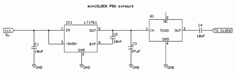
- the existing schematic is 2 clocks with a couple of inverters, etc (schematic attached)
- I attached the new clock signal to the track where the old clock was attached (this is some way away from the DIR chip it feeds) but there is nowhere safe nearer the DIR chip (circled on the schematic)
- The PS circuit is based on a low noise regulator so should be clean
- I'm taking a 5V feed from the DSP board as input to the voltage regulator & getting 3.3V out feeding the osc.
What am I doing wrong?
So here's why I asked - I expected a great improvement in the sonics when I replaced the existing clock signal with this osc fed with clean(?) PS. And I didn't hear any improvement!!
Here's the detail:
- clock is in on a dsp board in a Panasonic SA-XR57 (equibit) digital amp
- the few others who have changed this clock have reported great improvements
- the existing schematic is 2 clocks with a couple of inverters, etc (schematic attached)
- I attached the new clock signal to the track where the old clock was attached (this is some way away from the DIR chip it feeds) but there is nowhere safe nearer the DIR chip (circled on the schematic)
- The PS circuit is based on a low noise regulator so should be clean
- I'm taking a 5V feed from the DSP board as input to the voltage regulator & getting 3.3V out feeding the osc.
What am I doing wrong?
Attachments
Try to decouple the clock better. Use a 100nF cap right on the power and ground pins of the oscillator.
Why are you using a coupling cap on the clock output? Try driving the XTI pin on the controller through a 33R. Just like it shows the IC1005 pin 5 connected.
The 33r should be very close to the clock IC output. It is for damping reflections on the clock trace.
Solder the 33R directly to the clock output and then use a twisted pair for the clock. On the twisted pair's return current wire use the oscillator ground pin on the clock end, and on the load end solder to a ground close to where you attach the clock.
Hi, wildmonkeysects,
Thanks for the information. I see now why tiny mV ripple can make difference in clock performance.
Is this the reason why they make sinusoidal output osillator nowdays?
If the disturbance is from the trigger point (related to slope and rail voltage), will using a fast comparator (for replacing an inverter) with a reference made from simple voltage divider (between +rail and gnd) can make a better PSRR clock? That voltage divider will already include the supply ripple for trigger point.
Thanks again guys,
Rossl, I have a 100nF between + & gnd accross the smd clock. What I don't have is a 33R on the output of the clock. I will replace the output coupling cap with this 33R. Can't run twisted wire - have to use the existing track - nowhere safe to connect into!
Hi Lumanauw, I didn't need to remove the original clock & surrounding components - just disconnect it's output & connect mine in place
Chaos, complexity, and coherence
Yes, a sine osc, particularly a differential sine can have better power supply rejection. Can, as in doesn't always, but the potential is there. Once it is sliced into a "digital" square wave for cmos, the same issues of power/ground modulation of the trigger/transition time will apply, to a lesser degree. My experience is that even after passing through noisier gates, a clean source is still generally better...philosophically like starting with a clean source to see how it gets mucked up downstream...makes it easier to discern what happens than with a dirtier source.
I get the idea of cancelling power supply ripple/noise...however what you will have is a cycle by cycle shift, same as my example of a single logic gate sharing a power/ground. The relevant time frames are numbers of cycles corresponding to audible frequencies, and out of band frequencies that can fold back or intermodulate to the audible frequencies. The "jitter spectrum".
------
For jkenny:
It may be down to implementation and fine tuning to get audible benefits.
Are you physically close to the others who have done this mod to go listen and compare?
Also, is it clear that only one clock is needed for the functions you are using?
Cheers,
WMS
lumanauw said:Hi, wildmonkeysects,
Thanks for the information. I see now why tiny mV ripple can make difference in clock performance.
Is this the reason why they make sinusoidal output osillator nowdays?
If the disturbance is from the trigger point (related to slope and rail voltage), will using a fast comparator (for replacing an inverter) with a reference made from simple voltage divider (between +rail and gnd) can make a better PSRR clock? That voltage divider will already include the supply ripple for trigger point.
Yes, a sine osc, particularly a differential sine can have better power supply rejection. Can, as in doesn't always, but the potential is there. Once it is sliced into a "digital" square wave for cmos, the same issues of power/ground modulation of the trigger/transition time will apply, to a lesser degree. My experience is that even after passing through noisier gates, a clean source is still generally better...philosophically like starting with a clean source to see how it gets mucked up downstream...makes it easier to discern what happens than with a dirtier source.
I get the idea of cancelling power supply ripple/noise...however what you will have is a cycle by cycle shift, same as my example of a single logic gate sharing a power/ground. The relevant time frames are numbers of cycles corresponding to audible frequencies, and out of band frequencies that can fold back or intermodulate to the audible frequencies. The "jitter spectrum".
------
For jkenny:
It may be down to implementation and fine tuning to get audible benefits.
Are you physically close to the others who have done this mod to go listen and compare?
Also, is it clear that only one clock is needed for the functions you are using?
Cheers,
WMS
jkeny said:If I use a seperate PS does timing of power to OSC matter? Can it be powered up before AK4114 chip gets power?
You should try to power them up simultaneously if at all possible. The AK4114 unpowered probably looks like a couple of diodes to the supply rails and ground. (Substrate diodes- intrinsic or deliberate for esd protection or both..
") ) Perhaps not the best load to present to the output of your clock circuit.
) Perhaps not the best load to present to the output of your clock circuit.jkeny said:No possibility of damage to AK4114 chip? I don't think I can power-up at same time - amp PS is SMPS! I was thinking of running the clock off battery supply
Sure you can, just use a transistor to sense the other supply's output voltage and use that to turn on the supply to the clock.
- Status
- This old topic is closed. If you want to reopen this topic, contact a moderator using the "Report Post" button.
- Home
- Source & Line
- Digital Source
- I'm confused with Clocks