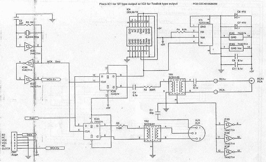
Hmm.. LC78601E has "Supply voltage selection input." in pin 2, but it's LC78601RE that is used in JVC. Apparently it outputs clock divided by 4 to this pin and it goes to CLK-pin in LA9242. It's "Reference clock input pin. 4.24MHz signal from the DSP is input."
Would it be better to divide external clock with flipflop or something else and put it to this pin? Does anyone have an oscilloscope? Just wondering..
Would it be better to divide external clock with flipflop or something else and put it to this pin? Does anyone have an oscilloscope? Just wondering..
I got mine from that guy. Smells like smoke, but it works.

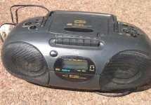
Jvc-rcez31 jvc-rcez32 jvc-rcez51
The EZ32 is not entirely compatible - apparently it takes a lot of extra work. See the posts by kevinkr.
Whilst waiting for parts to arrive so I can build the re-clocking board mentioned a few pages back in this thread, I stumbled upon this review of a CEC TL-1X transport:
CEC TL-1X
Looks to have more or less than same digital output board as Peter's TL0, but with the addition of an optical receiver too.
Scroll down about halfway and you can see the awful trace put out by the SPDIF signal from this board - this guy gets far better results from using the digital output 'direct' from the board and bypassing the output board.
Has anyone experienced a lack of bass who's DIY'd version of the CEC style digital output?
Cheers,
- John
The Lampizator was wrong: http://www.diyaudio.com/forums/digi...-improving-motor-cec-mabuchi.html#post1926921
Just read that thread - whew! Nice to know this was just a case of a faulty test then (one hope's he'll update his pages to reflect this...).
Looking forward to trying out this CEC-style reclocking board on my Shiga once the chips arrive. Only difference is I'll do it without the pulse transformer and instead use the 300/100 resistors. There's already a pulse transformer on the input of my DAC at any rate. Have heard many people don't like using pulse transformers, so I guess this is another avenue to experiment with.
- John
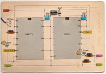
Wow I love that diagram - you must be a whiz at Photoshop? I'm currently doing an evening class studying beginners Photoshop actually, though will be a while before I produce work like that! Really helpful and makes it near enough foolproof to put one of these boards together - thanks!
Just curious why there's only one 33uF cap providing decoupling to both chips, whereas on the CEC circuit diagram I believe there is one cap per chip?
- John
Just curious why there's only one 33uF cap providing decoupling to both chips, whereas on the CEC circuit diagram I believe there is one cap per chip?
- John
P.S. I've probably missed a post somewhere that explains this, but according to Peter's circuit, plus Audio1st's, the digital output comes from pin 9 of the 74AS74. However according to the original CEC schematic it appears to come from pin 8...
Have I missed something?
Have I missed something?
Last edited:
I went with the actual CEC board, and the output comes from pin9, see post #12: http://www.diyaudio.com/forums/audio-sector/160373-cd-transport.html#post2069003
- Home
- Source & Line
- Digital Source
- Finally, an affordable CD Transport: the Shigaclone story