Bernhard said:
The crystal filter is rock steady. No jitter.
And filters with multiple crystals are even narrower
You just didn't have the idea
Maybe not. But I wonder why we can have a rock stable xtal filter but not a rock stable xtal oscillator.
Jan Didden
Provocative question: Is it really desirable to get rid of ANY jitter? I once did the following experiment: I produced white noise with Nyquist frequency in the audible range. Just interpolated there was clearly an audible tonal component. Various kinds of FIR filters that filtered out the Nyquist frequency reduced it more or less. A slight amount of phase noise (not visible in the plotted graphs of short samples) was able to remove it completely (with no filtering at all).
How I did this without having the same problem in the modulation noise would lead to far away from the topic.
How I did this without having the same problem in the modulation noise would lead to far away from the topic.
janneman said:
Maybe not. But I wonder why we can have a rock stable xtal filter but not a rock stable xtal oscillator.
Jan Didden
A precision xtal oscillator in a CDP is rock stable enough, but the LE signal after the SPDIF receiver is not.
Bernhard said:To shape the sine back to a square is no problem, use a precision comparator as done for example in a Kwak-clock.
I disagree, converting a sine wave back to a square wave almost always creates jitter. When a SPDIF signal is passed through a plastic fiber cable, the edges get quite slow (not as bad as a sine wave) it's the conversion back to a fast rise time that then adds one of the sources of jitter.
The jitter is the direct result of two causes; 1. Amplitude noise on the sloped edge of the slowed down signal and 2. Slicer uncertainty or internal comparator noise if you like that better. If we assume an error of +/- 1/2 LSB (redbook) we need a jitter value of 0.17 nanoseconds peak to peak (will someone check my math? It's late and I'm tired). I used 1/(2^16 times 44,100) and divided by 2 for 1/2 bit. Or we could say 85 picoseconds peak, 60 picoseconds RMS. Not easy IMHO.
I've experimented with using a crystal filter to clean up the awful output of a CMOS PLL chip. The two complement each other quite well; silicon VCO phase noise tends to be quite good narrowband but awful wideband, and a crystal will clear up the rest. The resulting spectrum is almost as good as a straight crystal VCXO.
However, crystal filters are *very* narrowband, the usable bandwidth is only a few KHz for a tens-of-MHz crystal. Temperature changes will move the center frequency around further than this bandwidth, and aging will likely push it outside over time. And if the input frequency isn't exactly in line with the crystal, like if you're using two different CDPs that are 100ppm off each other, it won't work unless you tune the filter whenever you change CDP's.
Crystal filters are something fun to play with. But IMO, a VCXO-based PLL is a better solution for phase noise performance, aging/temperature drift, etc.
Unfortunately, even if this were practical, in the course of creating your 'filter' what you end up doing is effectively creating a high 'Q' circuit whose intrinsic noise is lower than the original clock, and is in effect itself a low-jitter clock.
The basic illusion stems from the fact that people imagine that there is a high-purity sinewave 'lurking' in the jittery square clock waiting to be extracted, but there isn't.
There's no such thing as as free lunch.
Sorry
w
The basic illusion stems from the fact that people imagine that there is a high-purity sinewave 'lurking' in the jittery square clock waiting to be extracted, but there isn't.
There's no such thing as as free lunch.
Sorry
w
For Achieving what ? This is not for filtering a squarewave anymore.
Well, presumably you're going to tell us what it's for then... I mean, that's what you're trailering it for isn't it? And if it's not for filtering a squarewave then it's OT, what's it doing waking up this old dead thread?
w
Well, presumably you're going to tell us what it's for then... I mean, that's what you're trailering it for isn't it? And if it's not for filtering a squarewave then it's OT, what's it doing waking up this old dead thread?
w
Conditions have changed, I have put the clock inside the DAC and slaved the transport, there is no need to filter a squarewave anymore, all what would make sense is to further clean up the output of the sine oscillator before shaping it into a square.
After solving some problems, the crystal filter is now part of the Kwak clock, filter input connected to the coupling cap of the oscillator, filter output to the input of the comparator.
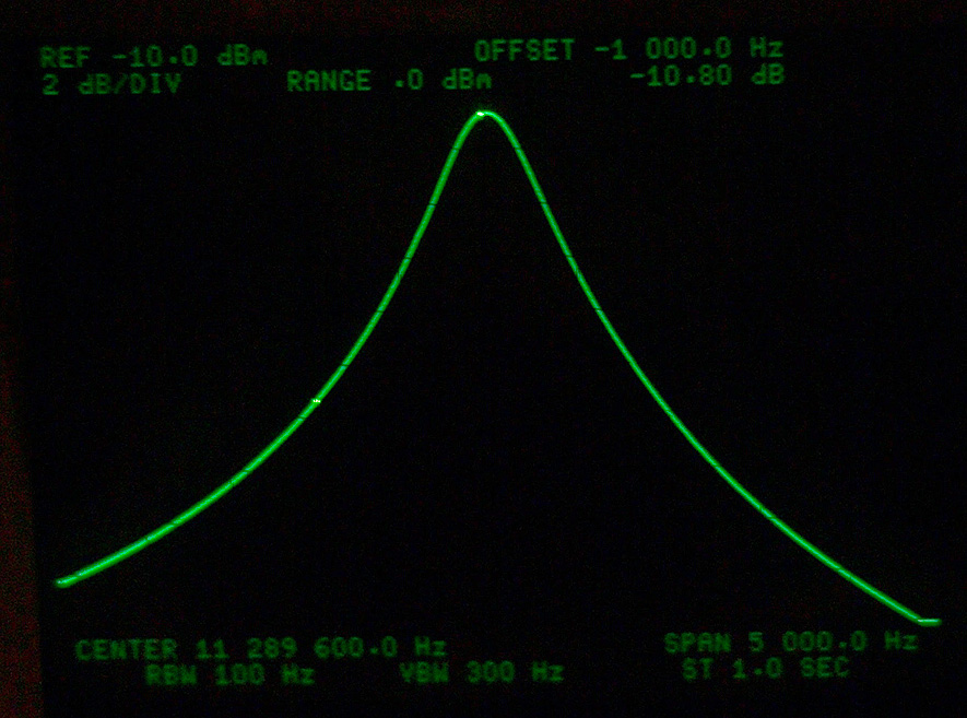
First, spectral analysis of the square output of the Kwak clock with no filter installed.
Please notice, the lines are not straight, it looks like there is a sine overlayed.
It looks different on every scan of the analyzer as if it moves along the line.
First, spectral analysis of the square output of the Kwak clock with no filter installed.
Please notice, the lines are not straight, it looks like there is a sine overlayed.
It looks different on every scan of the analyzer as if it moves along the line.
Last edited:
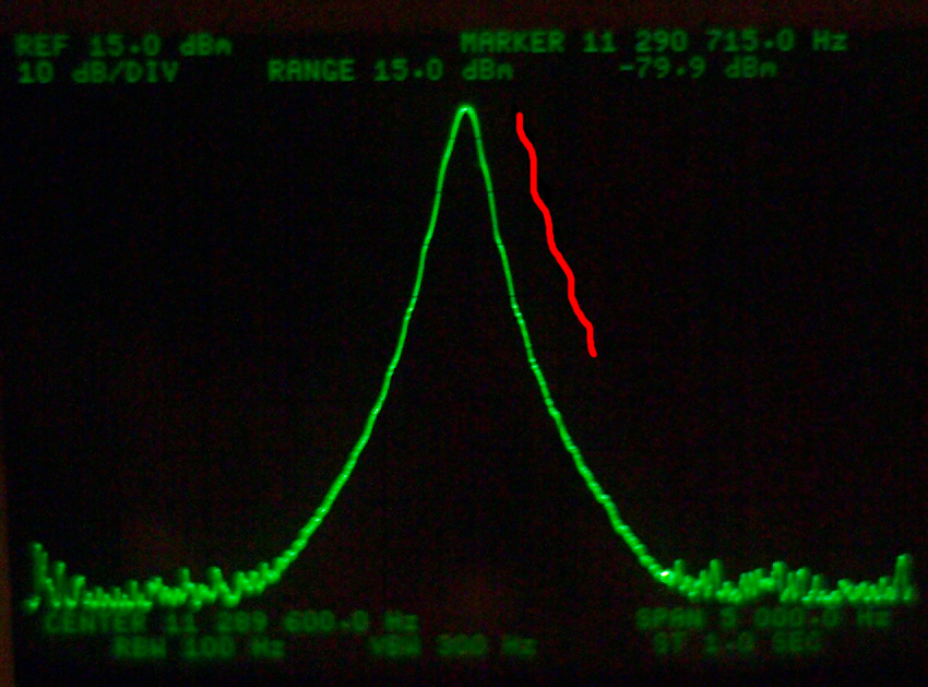
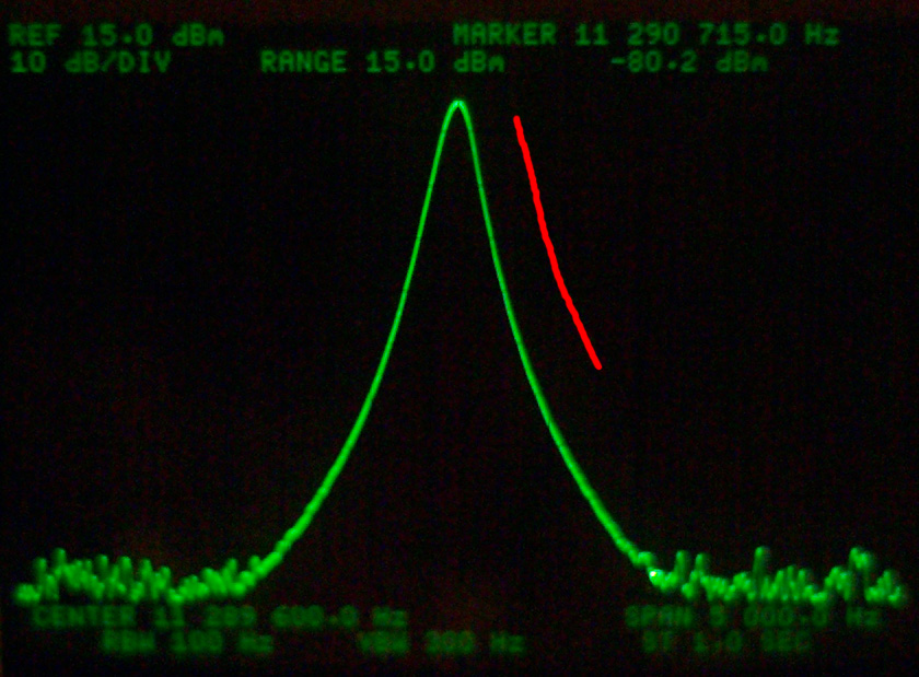
This is with the filter installed, the lines are straight.
Also in the lower part, there is less noise.
Next step would be a multi crystal filter.
I am not sure what is the cause of the flaws of the first waveform, I built the clock a few years ago on veroboard using point to point wiring, no ground plane and no shielding.
However the crystal filter is built the same way...
Last edited:
Hi Bernhard,
You already knows that
If there is no relation between LE and CLK, you mean that LE is an asynchronous input. It seems to be strange!
I think that LE is only an input, and critical signal still CLK.
Is there any other point of view?
Thanks
Here is a good solution, I have the same solution in my personal DAC: Jundac One.Conditions have changed, I have put the clock inside the DAC and slaved the transport...
You already knows that
Are you sure of that? Is LE not only an input synchronized with CLK signal?For example in my non-os DAC the jitter critical signal is LE...
If there is no relation between LE and CLK, you mean that LE is an asynchronous input. It seems to be strange!
I think that LE is only an input, and critical signal still CLK.
Is there any other point of view?
Thanks
Are you sure of that? Is LE not only an input synchronized with CLK signal?
If there is no relation between LE and CLK, you mean that LE is an asynchronous input. It seems to be strange!
I think that LE is only an input, and critical signal still CLK.
In the PCM1702 datasheet is stated that Iout changes on the fourth edge of the bitclock after LE.
For PCM56 there is nothing written like that.
Also the sound is clearly better with LE reclocking, compared to standard spdif.
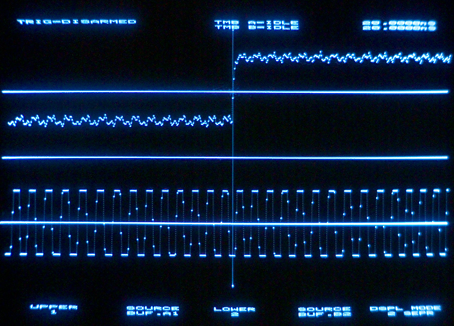
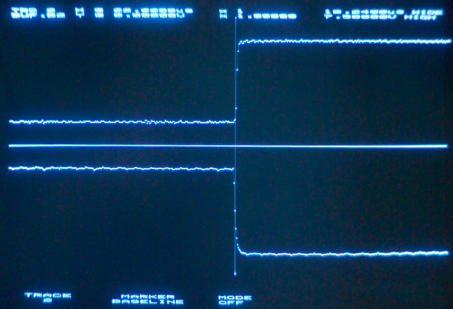
Look at the relationship Iout on upper trace with LE falling edge on lower trace.
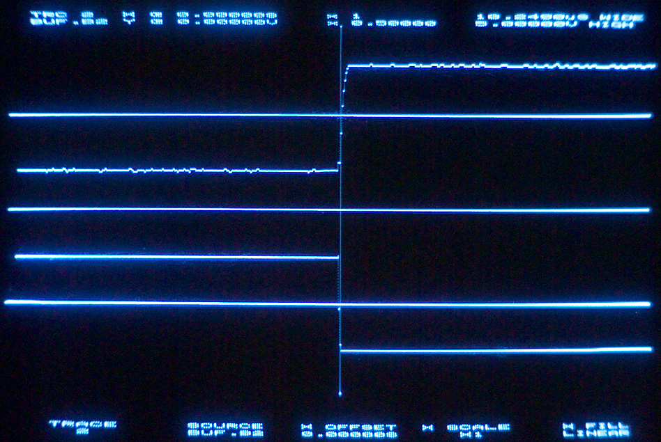
And Iout on upper trace with bitclock on lower trace.
From the cursor to the bitclock edges, left and right, is 40 ns each.
There is crosstalk inside the instrument unfortunately, spoiling the Iout trace, please ignore that ...
Hi Bernhard,
OK for picture 2 (Iout and CLK)
There is something strange in picture 1. Iout and LE start at the same time (red line on my picture). Iout starts before LE reach zero logic! It might have a short delay (few ns) at least.
In my personal DAC, I re-clock all signals (CLK, LE, DOR, DOL) with single chip (74xx574). It solves all time delay
Yes, and for the PCM1704, Iout occurs at the rising edge of the 2nd CLK.In the PCM1702 datasheet is stated that Iout changes on the fourth edge of the bit clock after LE.
For PCM56 there is nothing written like that....
OK for picture 2 (Iout and CLK)
There is something strange in picture 1. Iout and LE start at the same time (red line on my picture). Iout starts before LE reach zero logic! It might have a short delay (few ns) at least.
In my personal DAC, I re-clock all signals (CLK, LE, DOR, DOL) with single chip (74xx574). It solves all time delay
Attachments
There is something strange in picture 1. Iout and LE start at the same time (red line on my picture). Iout starts before LE reach zero logic! It might have a short delay (few ns) at least.
In my personal DAC, I re-clock all signals (CLK, LE, DOR, DOL) with single chip (74xx574). It solves all time delay
Second try, I use a 20 kHz sine for Iout and it depends a bit how I catch a bigger current step.
Also the first time one head was 1:1 and the other 1:10.
Still, the cable length is different about 40cm, lots of sources for uncertainty...
- Status
- This old topic is closed. If you want to reopen this topic, contact a moderator using the "Report Post" button.
- Home
- Source & Line
- Digital Source
- Idea for anti jitter filter