A bit off topic here, but here are the step by step instructions I compiled:
For me they worked, I had only one minor explosion")
INSTRUCTIONS
1) Determine operating voltage (Vload) and MAX load current (Iload). This come from your project, what do you want to power with the regulator?
2) If Vload>300 V and Vload < 400 V
Q2=MPSA94 or Toshiba A1626. NOTE that MPSA94 is NOT pin to pin compatible with MJE350. Some rework is needed
R3= 82K/5W
R4=220K/2W
If Vload< 300 V
Q2=MJE350
R3=56K/5W
R4=120K/2W
3) Iload+25mA < Iccs < 2 * Iload or 1.2 * Iload < Iccs < 2 * Iload
Vload + 25 V < Vccs < Vload + 50V
(NOTE: higher values of Iccs and vccs improve performances, but increase the heat production, I would start with a minimum needed difference between Iload and Iccs and vccs)
4) Make a first estimate of R1 using the following table
Iccs=40mA >>R1=56R/1W
Iccs=50mA >>R1=47R/1W
Iccs=60mA >>R1=33R/1W
Iccs=80mA >>R1=22R/1W
Iccs=100mA >>R1=20R/1W
5) Use PSU2 to determine the AC voltage needed considering the chosen topology of the filter. The transformer should be rated for 2 *Iccs.
If a center tapped transformer is used, populate only D10 and D12
If a normal transformer is used, install all the diodes and use the two contacts marked AC to connect the transformer. CT do not need to be connected
6) Set the trimmer R8 to 100 ohm
7) connect as dummy load (Calculate the value of the resistor Rdummy= Vload / Iload Wdummy= 2* Vload* Iload) I used some 20 K 20 W connected in parallel to adjust the values
8) connect two voltmeters, set on DC, one on the dummy load and one on R1, they will measure Vload and Vr1.
9) power the circuit (For a first test it can be safer to pre-heat the filaments, so that the load comes up faster)
10) with extreme care, and the left hand behind your back, adjust the output voltage to Vload.
11) Note the voltage Vr1 measured on R1 (should be in the range of few volts). The real Iccs can be calculated Iccs=Vr1/R1
12) Compare Iccs calculated with the project Iccs and reduce or increase the value (reducing R increase the current) so that they match. To do that iterate the process.
13) power off the circuit and wait for all the capacitor to discharge.
14) When Icss and Vload measured are OK, power off the circuit and wait for all the capacitor to discharge, disconnect the dummy load, disconnect the volt meters, and connect the real load.
HEAT DISSIPATION
Q1[mW] =Iccs * (Vccs-Vload) in any condition
Note (Vccs-Vload)< 200 V otherwise you fry Q1
Q3[mW] = 1.2 * Iccs * Vload when the regulator is unloaded (conservative in the worst case scenario. Avoid to operate the circuit without load, but the heat sink should be capable of the maximum dissipation, that can occur in case the load has a failure, e.g. burned filament )
Q3[mW] = (Iccs - Iload) * Vload when the load is draining current
NOTE 1: Current are expressed in mA, voltages in V and power in mW
NOTE 2: I you use a single heatsink for both components, you must electrically insulate them from the sink.
COMPONENT CHOICE
D9-D12 FRED diodes 1000 V 1A
R2 and R6 Carbon Composite (gate stopper)
Other resistors metal film, rated for 400 V
C2 and C3 WIMA MKP
C4 and C5 High ripple current, low ESR
R8 Multi turn trimmer, replace with a low ppm fixed resistor for final build
R4 Choose a resistor with low ppm as this is the voltage reference
TIPS
The pads are not tinned. To avoid oxidation put a thin layer of tin on them.
PLEASE NOTE THIS IS A DRAFT
Have fun,
D.
For me they worked, I had only one minor explosion
INSTRUCTIONS
1) Determine operating voltage (Vload) and MAX load current (Iload). This come from your project, what do you want to power with the regulator?
2) If Vload>300 V and Vload < 400 V
Q2=MPSA94 or Toshiba A1626. NOTE that MPSA94 is NOT pin to pin compatible with MJE350. Some rework is needed
R3= 82K/5W
R4=220K/2W
If Vload< 300 V
Q2=MJE350
R3=56K/5W
R4=120K/2W
3) Iload+25mA < Iccs < 2 * Iload or 1.2 * Iload < Iccs < 2 * Iload
Vload + 25 V < Vccs < Vload + 50V
(NOTE: higher values of Iccs and vccs improve performances, but increase the heat production, I would start with a minimum needed difference between Iload and Iccs and vccs)
4) Make a first estimate of R1 using the following table
Iccs=40mA >>R1=56R/1W
Iccs=50mA >>R1=47R/1W
Iccs=60mA >>R1=33R/1W
Iccs=80mA >>R1=22R/1W
Iccs=100mA >>R1=20R/1W
5) Use PSU2 to determine the AC voltage needed considering the chosen topology of the filter. The transformer should be rated for 2 *Iccs.
If a center tapped transformer is used, populate only D10 and D12
If a normal transformer is used, install all the diodes and use the two contacts marked AC to connect the transformer. CT do not need to be connected
6) Set the trimmer R8 to 100 ohm
7) connect as dummy load (Calculate the value of the resistor Rdummy= Vload / Iload Wdummy= 2* Vload* Iload) I used some 20 K 20 W connected in parallel to adjust the values
8) connect two voltmeters, set on DC, one on the dummy load and one on R1, they will measure Vload and Vr1.
9) power the circuit (For a first test it can be safer to pre-heat the filaments, so that the load comes up faster)
10) with extreme care, and the left hand behind your back, adjust the output voltage to Vload.
11) Note the voltage Vr1 measured on R1 (should be in the range of few volts). The real Iccs can be calculated Iccs=Vr1/R1
12) Compare Iccs calculated with the project Iccs and reduce or increase the value (reducing R increase the current) so that they match. To do that iterate the process.
13) power off the circuit and wait for all the capacitor to discharge.
14) When Icss and Vload measured are OK, power off the circuit and wait for all the capacitor to discharge, disconnect the dummy load, disconnect the volt meters, and connect the real load.
HEAT DISSIPATION
Q1[mW] =Iccs * (Vccs-Vload) in any condition
Note (Vccs-Vload)< 200 V otherwise you fry Q1
Q3[mW] = 1.2 * Iccs * Vload when the regulator is unloaded (conservative in the worst case scenario. Avoid to operate the circuit without load, but the heat sink should be capable of the maximum dissipation, that can occur in case the load has a failure, e.g. burned filament )
Q3[mW] = (Iccs - Iload) * Vload when the load is draining current
NOTE 1: Current are expressed in mA, voltages in V and power in mW
NOTE 2: I you use a single heatsink for both components, you must electrically insulate them from the sink.
COMPONENT CHOICE
D9-D12 FRED diodes 1000 V 1A
R2 and R6 Carbon Composite (gate stopper)
Other resistors metal film, rated for 400 V
C2 and C3 WIMA MKP
C4 and C5 High ripple current, low ESR
R8 Multi turn trimmer, replace with a low ppm fixed resistor for final build
R4 Choose a resistor with low ppm as this is the voltage reference
TIPS
The pads are not tinned. To avoid oxidation put a thin layer of tin on them.
PLEASE NOTE THIS IS A DRAFT
Have fun,
D.
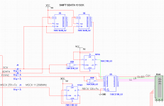
I took the ideas from Eric Juaneda's decoder and this is it (see attachment).Second option is to stop using any compensation and reclock using MCK from your I2S source to put everything in perfect sync. Good example would be Eric Juaneda’s decoder
The MSCK from 8414 which is Fsx256 is divided by two and it's used to latch all signals used by the AD. Everything is in perfect sync now.
As I will do my tests on perfboard I'm not sure the >11MHz MSCK will be happy. What do you think?
Thanks.
Attachments
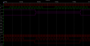
I'm using an evaluation Multisim 11 and the files sampler shared with us in post #233.What do you use to see the digital signals ?
D.
I took the ideas from Eric Juaneda's decoder and this is it (see attachment).
The MSCK from 8414 which is Fsx256 is divided by two and it's used to latch all signals used by the AD. Everything is in perfect sync now.
As I will do my tests on perfboard I'm not sure the >11MHz MSCK will be happy. What do you think?
Thanks.
Nice

Run a shielded wire as short as possible from 8414, center pin - MCK, shield - AGND. Connect only center pin at logic side, don't make any ground loops, should be ok then.
I have new up dat for AD1865:
http://www.diyaudio.com/forums/group-buys/155960-dac-end-andrea-ciuffoli-group-buys-169.html
http://www.diyaudio.com/forums/group-buys/155960-dac-end-andrea-ciuffoli-group-buys-168.html
http://www.diyaudio.com/forums/group-buys/155960-dac-end-andrea-ciuffoli-group-buys-167.html
http://www.diyaudio.com/forums/group-buys/155960-dac-end-andrea-ciuffoli-group-buys-169.html
http://www.diyaudio.com/forums/group-buys/155960-dac-end-andrea-ciuffoli-group-buys-168.html
http://www.diyaudio.com/forums/group-buys/155960-dac-end-andrea-ciuffoli-group-buys-167.html
It's nice that you removed the TL431 and used a separate salas reg for the analog part of the CS8141. I also like that the psu and dac are on the same boardI have new up dat for AD1865
Even if not asked I will say what I would have done:
- on DAC side: which is more important, I would have used smds for the CS PLL part (as in CS8416 data sheet) and solder the CS directly to the DAC board.
- on the PSU side: in my opinion, only one Salas reg would have been more than enough for the digital part, or even a simple LT1086. This would reduce board size and costs.
Davide,
You could also buy one from TP TOSLINK Optical Input Module
Fairly priced and needs only +5 to 12VDC and GND
You could also buy one from TP TOSLINK Optical Input Module
Fairly priced and needs only +5 to 12VDC and GND
Anyone try a small film at C30?
I've been doing a lot of research and C30 seems to be the most important cap for SQ. I talked to a couple excellent dac designers who both said a small film cap there would be excellent.
They also said triple bypass should create excellent results meaning small film bypassed with a good electrolytic bypassed with a small film.
C30? In which schematic??
Davide,
You could also buy one from TP TOSLINK Optical Input Module
Fairly priced and needs only +5 to 12VDC and GND
Actually is exactly what I have, it works just connecting it to the SPDIF input of the DAC-END board, but I am not sure it is the right way to connect it.
This module has only a small regulator on board, the output of the connector goes directly out.
Thanks,
D.
C30? In which schematic??
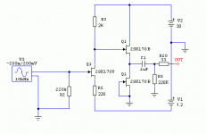
I guess its in the original schematic. Its the cap that feeds the 1865

One friend say about The DAC-END
**After purchasing the DAC-end kit from Quanghao, I absolutely felt that this an excellent DIY DAC. You know how my feeling at the time when I first heard the organic sound from it? I played 3 CDs straight to 1AM. The more I listened, the better the sound is.
Music is soooo smooth. Bass is very tight and deep, high is transparent and sparkling, and the vocal of The Carpenter is, OMG, absolutely stunning! Really out of this life.
After a couple of weeks, we had a mini comparisons between Dac-End 2 and Audio Research DAC and CDP TEAC 50. To my own taste, the DAC-End has smoother, more transparent and organic sound. It has the most life-like representation that I've ever heard. ***
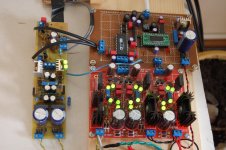
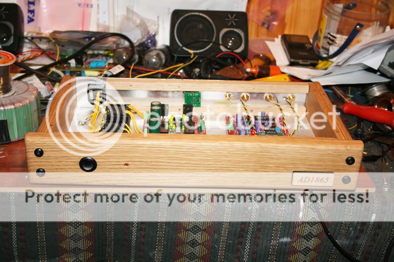
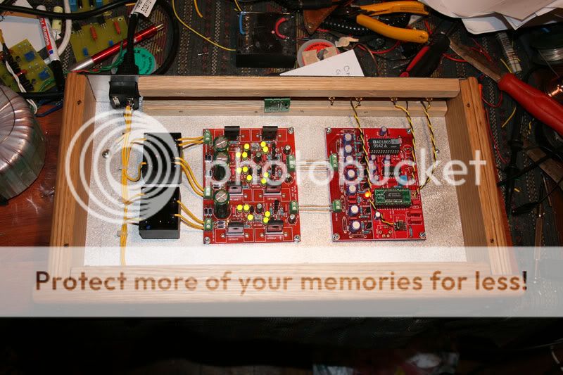
In the meantime I finished my test AD1865 DAC as well
It uses only an inverter to latch the LR and LL as Andrea did.
The digital power supply is with an LM317 with very good filtering, the rest use Salas shunts. The CS8414 has the PLL fllter components and small decoupling caps soldered directly to its pins
The preamp on the left is based on this Juma's preamp link but slightly modified as in the attached image, to get 1V RMS out (kinda JBoz with B1 buffer).
All in all I'm very happy with the results.
As comparison is rooted deep in our souls, after some happy listening hours I started to compare it to my cd player, which is a modest Exposure 2010S. Both DAC and CDP have 1V rms out so with a switch I can change on the fly.
Hmmm... what can I say, it's not night and day situation, actually I couldn't make a clear difference between them. The DAC is just a bit smoother and maybe it's imaging is a bit better, also listening to an orchestra I feel that the instruments are better placed in space.
btw... my other components are a Quad 405 DCD-Mod3 and a JMLab Cobalt 816S
I think this is similar to wine tasting, you either learn it or go to a wine tasting trip or just unknowingly enjoy it.
This is not the end yet... I started the PCB design for an I2S capable board. It will have CS8414, I2S shifter with I2S from either the CS or an external source and the AD. This (dev)board will also contain the plain inverter on it to have a comparison base of I2S shifted CS. As I'm doing it in my work time don't expect to be ready on schedule
After the above board is ready I would like to try to marry the AD with a Pass D1 I/V, but fall will come I believe until I will do that.
Cheers.
Attachments
Last edited:
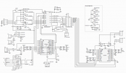
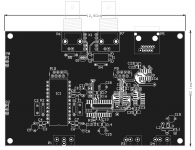
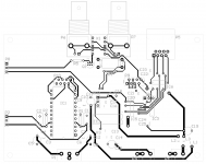
DAC v0.5
Hi!
I've been working with a snail pace on a DAC development board based on AD1865. I call it a development board as it contains daughter board connectors to try different AD1865 format converters.
It contains the followings:
- AD1865 using passive I to V conversion as Audiodesign/Quanghao did
- SPDIF receiver based on CS8414
- 2 X relayed SPDIF inputs using BNC connectors
- AD format converter board connectors (see below)
- I2S buffered input using RJ45 connector
- Multiplexer IC to choose between I2S or SPDIF
- Input selector to choose from I2S or SPDIF
- Input selector to choose SPDIF 1 or 2
- Separate supply inputs for analog AD1865, analog CS8414 and a single common digital supply input
- Jumper selector to select CS8414 output format LSBJ or I2S
- Jumper selector to select in phase/out phase data
- Common top ground plane. Although the ground plane is common for analog and digital side I tried to partition the board to have analog ground at the bottom part and digital ground at the top
The daughter board that will be connected between P9 - P10 (in 90 degree angle) might contain from a simple inverter (to match LSBJ signals from CS8414 to AD1865) to a fully featured I2S converter.
As I'm new in high speed PCB design please help me with your ideas about what should be done to have a good DAC board at the end.
Thanks,
Zsolt
Attachments
Last edited:
- Status
- This old topic is closed. If you want to reopen this topic, contact a moderator using the "Report Post" button.
- Home
- Source & Line
- Digital Source
- AD1865 the best DAC