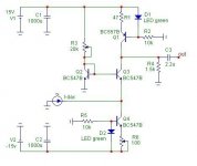
Built this the last week; it's a variation of Jocko's simple I/V, using all generic unmatched parts, larger bias currents, and the R4 upstream of C3.
This is used in a non-oversampling cd player with Kwak-Clock version 3 and TDA1541A-S1.
I have adjusted Vc(Q3) with pot R6 to 10.0 Vdc
Ve(Q3) is adjusted with pot R3 to 0 Vdc, and readjusted after a few hours. It doesn't change much over time, within +/-1.0mV.
Current source Q1 is about 23mA, of which 6mA flows into R4, 17mA through Q3 and 15mA through current sink Q4.
All bjt's have hfe of ca. 300-400 measured with multimeter.
Since I didn't measure Vbe on Q3 and Q2 I ended up with different R3 values; ca. 5.6k and 22k.
I suppose one could select to get the lowest R3 value, that is, have some moderate current flowing into Q2.
The sound ?
Well my previous I/V was a LM6172 opamp driving a J309 jfet biased by few mA, Riv between +V and fet's drain.
Later I replaced the J309 by a BS170 mosfet which has higher transconductance, hence less "correction" to be done by opamp on fet's gate to keep output voltage compliance of 0V.
The latter sounded more sweet, treble got more transparant.
Just last week I replaced the BS170 with a BC547B and it sounded a little better again, so I decided to built this circuit.
Got an improvement again; sounds like treble is more free and transparent and basses seem to be driven by some "mass".
This circuit can be universally used for other current output DAC's;
use pot R6 to get the wanted Vce on Q3.
To use it with Philips DACs like the TDA1543 and TDA1545A with DC voltage on output, replace Q2 with LED's, zener, or diodes to get stay within the valid DC compliance range.
I do have some SA970's and SC2240's to try, which might sound better...but even with generic parts it sounds pretty good.
Have fun,
Attachments
Nice to see someone else tried Jocko´s circuit.
I have tried a similar in a DAC with PCM63´s,but with 2SA970´s & 2SC2240´s.
I have put a capacitator in parallell to R4 as a filter and all is followed with a simple JFET follower(2SK170).
It sounds really good,better then the previous analog stage which was the usual opamp style.
Nicke
I have tried a similar in a DAC with PCM63´s,but with 2SA970´s & 2SC2240´s.
I have put a capacitator in parallell to R4 as a filter and all is followed with a simple JFET follower(2SK170).
It sounds really good,better then the previous analog stage which was the usual opamp style.
Nicke
Hi,
You may wish to consider cascoding both the current source (load)transistor AND the current conveyor transistor and to use a lot of voltage in the "+B"....
BTW, the same principle of course works great with valves too....
Sayonara
rbroer said:I do have some SA970's and SC2240's to try, which might sound better...but even with generic parts it sounds pretty good.
[/B]
You may wish to consider cascoding both the current source (load)transistor AND the current conveyor transistor and to use a lot of voltage in the "+B"....
BTW, the same principle of course works great with valves too....
Sayonara
tweaks
Try replacing the LEDs with three signal diodes. Try fixed resistors instead of pots once you have figured out the value needed. Try changing the 10K bias resistors (currently used on LEDs) to 20K and putting them to the opposite power supply rail instead of to ground. If you do any of these mods, let us know what you hear. To me LEDs and pots are extremely non-linear (noisy and distorted).
Ric Schultz
Cascoding:
Yes, I've been thinking to make the constant current source a little better by cascoding, but, higher B+ are hard to find in cd players (this is not a standalone DAC). Dunno if there will be audiable gains though.
A next version shall use a SA970 as CB, so I can cascode the current sink with a J111 fet.
What is the benefit of cascoding the current conveyor transistor ?
Then the cascode transistor will have the "problem" of a variable collector voltage.
LEDs & pots:
Really ? In fact I did some measurements last week, comparing how different LEDs and three 4148 change their voltage with increasing current. Red was best, green next, yellow changes a lot, like the three diodes. As a reference for a BJT CCS I suppose the steadier, the better.
Many other inmates seem to be using them.
But I'll compare LED/diodes on the pcb version I'll be using on a cd player with the TDA1543 (this was just a quick prototype).
A hunch tells me you already know the outcome Rick ?
Indeed those resistors on the LEDs can be connected to the opposite rail. One can even save a resistor by connecting the upper LED in series with 18k and next in series with the lower LED.
Happy new year to y'all.
Attachments
Hi,
For a higher +B simply build an external supply and while you are at it also make seperate suppies in the same case for clock and DAC, leaving only servo and uP powered from the internal supplies.
The changes in collector voltage change the transfer curve of the Transistor. If you "nail down" this voltage via a cascode you much reduce this effect. Same goes for FET's and Valves.
If you then use a suitably high voltage cascode transistor (or better FET, Valve!?) you can use a very high Supply Voltage which increases headroom and helps to keep the modulation of the Collector/Emitter or Drain/Source Voltage in percent of the absolute voltage small.
My Final Gambit would then be a suitable output transformer driven by the cascode and directly into a suitably low load...
I do agree on the pot's (but that should be self evident), on the LED Front, why not use a TL/LM431 instead, it costs more than LED's or diodes but is best in the context and for a DIY Unit....
Also, feed references NOT via resistors but via current sources, J-Fet "constant current diodes" or selected J-Fets tend to work fine...
Later T
rbroer said:Cascoding:
Yes, I've been thinking to make the constant current source a little better by cascoding, but, higher B+ are hard to find in cd players (this is not a standalone DAC).
For a higher +B simply build an external supply and while you are at it also make seperate suppies in the same case for clock and DAC, leaving only servo and uP powered from the internal supplies.
What is the benefit of cascoding the current conveyor transistor ?
Then the cascode transistor will have the "problem" of a variable collector voltage.
The changes in collector voltage change the transfer curve of the Transistor. If you "nail down" this voltage via a cascode you much reduce this effect. Same goes for FET's and Valves.
If you then use a suitably high voltage cascode transistor (or better FET, Valve!?) you can use a very high Supply Voltage which increases headroom and helps to keep the modulation of the Collector/Emitter or Drain/Source Voltage in percent of the absolute voltage small.
My Final Gambit would then be a suitable output transformer driven by the cascode and directly into a suitably low load...
LEDs & pots:
I do agree on the pot's (but that should be self evident), on the LED Front, why not use a TL/LM431 instead, it costs more than LED's or diodes but is best in the context and for a DIY Unit....
Also, feed references NOT via resistors but via current sources, J-Fet "constant current diodes" or selected J-Fets tend to work fine...
Later T
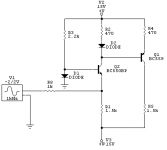
Hee.....this IV-stuff just keeps coming back.. great ... I use a very simple IV stage with 1 BJT, 1 diode, 1 cap and 3 resistors.. and it works just fine..... better than passive IV with just a resistor I think.. but how about this one .. DC to 10MHz.... better put some LP in it somewhere..nice output of 2Vrms too .. and low distortion.. but propably needs very good supply... all simulated offcourse (if you know me ") )...
)...
best of new years greetings,
Thijs
)...best of new years greetings,
Thijs
Attachments
AMT-freak said:[B
@Nicke:
Could we have a look at your circuit?
[/B]
It is almost the same as Jocko published but without the coupling cap.
And it is followed with a JFET source follower.
I don´t want to publish yet,because I got some clues from Jocko in a private email to him and it is his decision to publish it.
If you read the whole thread you could figure it out myself.
Why don´t you try the published circuit to start with?
I am very satisfied with my I-V stage.
A last hint:Look at Nelson´s SU-SY patent.
jkeny:
Dunno, never used the IRF610 since inmate Dave from downunder compared it to BJT, and latter sounded and measured better.
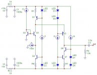
After all suggestions I've come up with a version I'll try next (still enjoying the 1st version though);
I added a PNP cascode on the current conveyor to keep it's Vce pretty constant and as a bonus it creates more Vce voltage headroom on Q5 since it's referenced to negative rail.
I have cascoded current sink Q7 with Q6 since this one will be "seeing" the output voltage swing.
I1 ~ I4 are constant current sources made of jfets with resistor.
I'll be using 2SA970´s & 2SC2240´s
bias Q3, Q5 = 15mA
Vce(Q5) = 19V,
Ve(Q5) = 11V,
Vc(Q5) = -8V (+/-3V signal swing)
Any suggestions for a "bigger" Q5 ?
I may add the Borbely follower with two 2SK170 BL's
Regards,
Dunno, never used the IRF610 since inmate Dave from downunder compared it to BJT, and latter sounded and measured better.
After all suggestions I've come up with a version I'll try next (still enjoying the 1st version though);
I added a PNP cascode on the current conveyor to keep it's Vce pretty constant and as a bonus it creates more Vce voltage headroom on Q5 since it's referenced to negative rail.
I have cascoded current sink Q7 with Q6 since this one will be "seeing" the output voltage swing.
I1 ~ I4 are constant current sources made of jfets with resistor.
I'll be using 2SA970´s & 2SC2240´s
bias Q3, Q5 = 15mA
Vce(Q5) = 19V,
Ve(Q5) = 11V,
Vc(Q5) = -8V (+/-3V signal swing)
Any suggestions for a "bigger" Q5 ?
I may add the Borbely follower with two 2SK170 BL's
Regards,
Attachments
i did post some wrong info about 2SC2240 and 2SA970. The 2240 can easyli be used up to around 30mA but the complementary 970 starts rolling off at around 10mA.
I have a suggestion :
Design a complementary I/V stage. Does not have to use more than 4 BJT's in the active stage.
pro's :
Lower input impedance the half of a single BJT.
DAC see's a constant impedance.
I have a suggestion :
Design a complementary I/V stage. Does not have to use more than 4 BJT's in the active stage.
pro's :
Lower input impedance the half of a single BJT.
DAC see's a constant impedance.
Sonnya,
check the other I/V thread ... there you can the my efforts in designing complementary I/V stage. .. simulated great!
That other guy found a way optimize the canceling of the 2nd harmonic distortion, allthough he says it not a slightly different way and makes it look like something bad...
check the other I/V thread ... there you can the my efforts in designing complementary I/V stage. .. simulated great!
That other guy
found a way optimize the canceling of the 2nd harmonic distortion, allthough he says it not a slightly different way and makes it look like something bad...Hi,
Well, in that case, why not use a transconductance cell on a chip ("diamond transistor") like the OPA660? There you have already perfectly matched transistors on one chip, a buffer and can be run open loop. I think AD also has a transconductance Op-Amp (743? not sure) where the transconductance node is available externally and that can be used open loop thusly....
Of course, that replaces all that lovely discrete stuff with a chip and a few resistors but it will sure sound better AND measure better than all that cludge, but it would go against the DIY Spirit. Anyway, these days it is VERY HARD to make discrete designs that are even competetive against competent implementations of the right type of chip, but that's just me.
Sayonara
I have a suggestion :
Design a complementary I/V stage. Does not have to use more than 4 BJT's in the active stage.
pro's :
Lower input impedance the half of a single BJT.
DAC see's a constant impedance.
Well, in that case, why not use a transconductance cell on a chip ("diamond transistor") like the OPA660? There you have already perfectly matched transistors on one chip, a buffer and can be run open loop. I think AD also has a transconductance Op-Amp (743? not sure) where the transconductance node is available externally and that can be used open loop thusly....
Of course, that replaces all that lovely discrete stuff with a chip and a few resistors but it will sure sound better AND measure better than all that cludge, but it would go against the DIY Spirit. Anyway, these days it is VERY HARD to make discrete designs that are even competetive against competent implementations of the right type of chip, but that's just me.
Sayonara
tschrama said:Sonnya,
check the other I/V thread ... there you can the my efforts in designing complementary I/V stage. .. simulated great!
That other guy
Yes i have read it. Add a folded cascode as you mentioned instead of your caps in the collectors. When modifyed this circuit could easely work with PCM1738... I know i know this is not part of this thread.
By the way. Use Switchercad III from linear tech. with this simulator you won't get fantastic distortion levels.
My circuit measure around -92dB based on the modified Jocko circuit first posted from Rbroer but with theoreticly current sinks and sources!
if i interchange them with fet's or BJT the numbers get 10dB higher.
Hi,
Not off-hand, but it really should be obvious from the Datasheet. Here the basics for the OPA660.
You connect a 270 Ohm resistor for biasing from pin 1 to the negative rail.
You decouple the negative and positive rail (pin 4 negative and Pin 7 positive) well and according to RF principles to ground, supply +/-5V.
You connect pin 3 via 100 Ohm to ground and pin 2 to the current input from the DAC. You place the required I/V conversion resistor on pin 8 and link pin 8 via a 100 Ohm resistor to pin 5.
Buffered output is from pin 6 via a 51 Ohm Build out resistor.
This has no lowpass, I would recommend a 62nF capacitor to ground on the output, this forms with the 51 ohm build out resistor a 50KHz 1st order lowpass, sufficient if the DAC is operated with 4 Times oversampling or more. You could make the Filter 2nd Order by paralleling the I/V resistor with a suitable value capacitor. The requirements for filtering for non oversampling operation are controversial, many people have their own ideas, as do I.
With -4mA Peak current from a TDA1541 the I/V conversion resistor should be sized so that the typhical output Voltage compliance is not exceeded or a +2mA compensating current should be injected into the TDA1541 Output. This is done easiest by using a 2k4 Resistor from a Well filtered +5V supply via a further 100ohm/1,000uF Filter section.
In this case the compensating current is used we have +/-2mA full scale peak current out of pin 8. To get 2.8V Peak (2V RMS) we thus need a 1k4 resistor, nearest standard value is 1k5 so we use that from pin 8 to ground. For a 50KHz 2nd Order lowpass we use a 33nF capacitor on the output and a 1nF capacitor in parallel to our 1k5 I/V conversion resistor.
I would feel that shunt regulating the +5V and -5V supplies via TL431/LM431 Shunt regulators is highly desirable.
L8er T
please could you make a simple example schematic...
Not off-hand, but it really should be obvious from the Datasheet. Here the basics for the OPA660.
You connect a 270 Ohm resistor for biasing from pin 1 to the negative rail.
You decouple the negative and positive rail (pin 4 negative and Pin 7 positive) well and according to RF principles to ground, supply +/-5V.
You connect pin 3 via 100 Ohm to ground and pin 2 to the current input from the DAC. You place the required I/V conversion resistor on pin 8 and link pin 8 via a 100 Ohm resistor to pin 5.
Buffered output is from pin 6 via a 51 Ohm Build out resistor.
This has no lowpass, I would recommend a 62nF capacitor to ground on the output, this forms with the 51 ohm build out resistor a 50KHz 1st order lowpass, sufficient if the DAC is operated with 4 Times oversampling or more. You could make the Filter 2nd Order by paralleling the I/V resistor with a suitable value capacitor. The requirements for filtering for non oversampling operation are controversial, many people have their own ideas, as do I.
With -4mA Peak current from a TDA1541 the I/V conversion resistor should be sized so that the typhical output Voltage compliance is not exceeded or a +2mA compensating current should be injected into the TDA1541 Output. This is done easiest by using a 2k4 Resistor from a Well filtered +5V supply via a further 100ohm/1,000uF Filter section.
In this case the compensating current is used we have +/-2mA full scale peak current out of pin 8. To get 2.8V Peak (2V RMS) we thus need a 1k4 resistor, nearest standard value is 1k5 so we use that from pin 8 to ground. For a 50KHz 2nd Order lowpass we use a 33nF capacitor on the output and a 1nF capacitor in parallel to our 1k5 I/V conversion resistor.
I would feel that shunt regulating the +5V and -5V supplies via TL431/LM431 Shunt regulators is highly desirable.
L8er T
Got it, thanks!
Nice interesting datasheet... I always love those simplified circuit diagrams.. Maybe use BUF634 instead of the 'onboard buffer' and connect direct to your favorite headphone
gr,
Thijs
PS
I'm still trying to make a perfect, ultra low noise, super fast V/I convertor (1-2mA max)at here at my work (Phd student). Wouldn't this opa660, with emmitor degeneration do this job?
- Status
- This old topic is closed. If you want to reopen this topic, contact a moderator using the "Report Post" button.
- Home
- Source & Line
- Digital Line Level
- Simple I/V for TDA1541