Hi Alexandre,
You need roughly 1 ... 2Vpp trigger signal amplitude for reliable triggering. This will inject considerable switching noise.
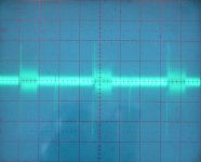
I attached a close up of the Simultaneous interface switching noise that manages to leak to the TDA1541A output. This is an amplified TDA1541A output signal.
I have 1K series resistors on DOL, DOR, and BCK. LE is directly injected for lowest trigger uncertainty.
You can see the 16 bit data burst & bit clock noise (the spikes you see in the low level measurement). Then 16 bit silence (no bus activity), we can see that ground-bounce now reaches zero.
Then the outputs are latched with LE (spike) followed by 48 bits silence. Then the next sample is clocked in the same way.
We would get similar extra switching spikes on the output when triggering the DEM oscillator with 1 ... 2Vpp.
With 50Hz DEM we have one switching spike every 882 samples. With 200 KHz DEM we have 4.5 spikes in each sample. This illustrates the impact of high DEM clock rates, every sample is distorted by the spikes generated by the free running 200 KHz DEM clock regardless of decoupling. This is switching noise (ground-bounce) generated on the chip, out of reach for external corrections.
The TDA1541A is based on -silent- current steering logic (comparable with ECL). So it won't get much better using modern CMOS logic that produces more switching noise compared to ECL.
John, if one wishes to experiment with synchronous DEM clock would there be any benefit in using an attenuator before the DEM pin (like the ones used for the I2S inputs)?
You need roughly 1 ... 2Vpp trigger signal amplitude for reliable triggering. This will inject considerable switching noise.
I attached a close up of the Simultaneous interface switching noise that manages to leak to the TDA1541A output. This is an amplified TDA1541A output signal.
I have 1K series resistors on DOL, DOR, and BCK. LE is directly injected for lowest trigger uncertainty.
You can see the 16 bit data burst & bit clock noise (the spikes you see in the low level measurement). Then 16 bit silence (no bus activity), we can see that ground-bounce now reaches zero.
Then the outputs are latched with LE (spike) followed by 48 bits silence. Then the next sample is clocked in the same way.
We would get similar extra switching spikes on the output when triggering the DEM oscillator with 1 ... 2Vpp.
With 50Hz DEM we have one switching spike every 882 samples. With 200 KHz DEM we have 4.5 spikes in each sample. This illustrates the impact of high DEM clock rates, every sample is distorted by the spikes generated by the free running 200 KHz DEM clock regardless of decoupling. This is switching noise (ground-bounce) generated on the chip, out of reach for external corrections.
The TDA1541A is based on -silent- current steering logic (comparable with ECL). So it won't get much better using modern CMOS logic that produces more switching noise compared to ECL.
Attachments
From what I know, the basic DEM oscillator is based on a FlipFlop (Multivibrator): https://upload.wikimedia.org/wikipe...or.svg/220px-Transistor_Multivibrator.svg.png
If we assume that C1 is the cap that is accessible over the Pinout, I could imagine that you'd only need to bias the base of transistor T2.... But that is only my guessing.
If we assume that C1 is the cap that is accessible over the Pinout, I could imagine that you'd only need to bias the base of transistor T2.... But that is only my guessing.
DEM, Simultaneous protocol converter
Hi John,
what family did you use for the single gates 74LVC1Gxx ??
In the present DEM I use 470n SMD film CAPS soldered directly under
the TDA1541A chip. When changing to 50Hz-DEM with 100uF-Elkos
is it better to remove the 470n film caps or keep them in parallel.
Thanks
Hi John,
what family did you use for the single gates 74LVC1Gxx ??
In the present DEM I use 470n SMD film CAPS soldered directly under
the TDA1541A chip. When changing to 50Hz-DEM with 100uF-Elkos
is it better to remove the 470n film caps or keep them in parallel.
Thanks
From what I know, the basic DEM oscillator is based on a FlipFlop (Multivibrator): https://upload.wikimedia.org/wikipe...or.svg/220px-Transistor_Multivibrator.svg.png
If we assume that C1 is the cap that is accessible over the Pinout, I could imagine that you'd only need to bias the base of transistor T2.... But that is only my guessing.
Thanks for this..
WRT the linked diagram, the connecting pins are for DC voltage supply to the circuit, which is different from what is happening at pins 16,17 of 1541A.
Given the scarcity of 1541A's, that 16 and 17 to -15V via 6k8 (ea) works, and has both parts of that circuit at the same potential, I'd like to be sure about what is actually going on before blindly leaping toward an 'improvement'.
Perhaps John could elaborate for peace of mind..
Thanks.
You can see the 16 bit data burst & bit clock noise (the spikes you see in the low level measurement). Then 16 bit silence (no bus activity), we can see that ground-bounce now reaches zero.
Then the outputs are latched with LE (spike) followed by 48 bits silence. Then the next sample is clocked in the same way.
This was interesting to see. Was that measurement done by probing directly at the I/V resistor, or with an amplifier?
I wonder if an even cleaner analog output could be obtained with something like the I/V I recently posted. Where the I/V resistor is referenced to +5V. The probe ground must be connected to +5V, of course.
Thanks,
Alex
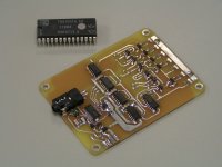
And now the practical 24 bit Left Justified to Simultaneous protocol converter circuit.
With LJ format the Right channel data is present when WS is low and the Left channel data is present when WS is high. With I2S the Left channel data is present when WS is low and the Right channel data is present when WS is high.
The 24 bit left justified interface signals DI (Data Input), WSI (Word Select Input), and BCKI (Bit Clock Input) enter the circuit at the top left.
First we have to identify and invert the MSBs. With LJ format we know that the MSB comes immediately after a WS change. U1, U2, and U9 create a delay that equals exactly one bit.
This works as follows, U1 delays the WSI signal for half a BCKI clock period. U2 receives an inverted BCKI signal and delays WSI for another halve BCKI clock period. Total delay is now -exactly- 1bit.
When we XOR this signal (U2 pin 4) with WSI we get a positive pulse the moment MSB occurs in the stream, immediately after a WSI change.
XOR gates can be used to invert a signal. When we put a "1" on the control input the signal on the other input is inverted. When we put a "0" on the control input the signal on the other input is not inverted.
When we XOR this pulse with the DI signal we can invert MSB only as the inversion only occurs during the short moment the MSB identifier pulse goes high. I combined two XOR gates by using a 3 input XOR gate. If this is a problem one can combine U2 Q output with WSI in a 74HC86 and then combine the output of this 74HC86 with DI using a second 74HC86 XOR gate. The output of that second XOR gate is connected to U3 D input.
Ok so we inverted MSB on the fly for both L and R channels.
We will need data delay circuits and in order to phase align both L and R channel data we start with flip-flop U3 so we can clock out both L and R channel data on the same BCKO clock edge.
We now have the DOR signal present on U3 pin 4.
The Left channel can now be aligned by adding 32 bit delay (U5 ... U8) and now we have DOL data on U8 pin 13.
The remaining thing to do is disabling DOL, DOR, and BCKO for the remaining 48 bits.
U4 is a counter that only counts when WSI is low (RST = 0) After 16 pulses its output Q4 (pin 5) goes high and when we NOR this signal with WSI we get a window signal that is only "1" when the 16 data bits are clocked out.
This window signal drives 3 AND gates U12, U13, and U14 that force these signals to "0" after the 16 bits have been clocked out.
The WSI signal is simply fed through and occurs at the output as the LEO (Latch Enable Output) signal that latches the TDA1541A outputs (simultaneous mode) on the -rising- edge of BCK.
The circuit consumes very little power, simple LED (L1) and diode(D1) shunt offer approx. 2.4V supply voltage (VDD) so we don't need attenuator circuits and we have low switching noise in the protocol converter circuit.
Hi ecdesigns,
I confuse ICs with ICs in your picture (http://www.diyaudio.com/forums/atta...ding-ultimate-nos-dac-using-tda1541a-pcv1-jpg)
Could you help correct my list of ICs
1) U1, U2, U3 (74G79) can be The D-type Flip Flop MC74HC74A from ON Semiconductor
2) U9 (74G04) can be the Hex Inverter PO74G04A from PotatoSemi
3) U12, U13, U14 (74G08) can be the positive-AND gate PO74G08A from Potato Semiconductor
4) U10 (74G386) can be the Exclusive OR Gate 74HC86 from PotatoSemi
5) U4 (74HC4060) can be the 14-stage binary ripple counter with oscillator 74HC4060 from Nexperia
6) U5, U6, U7, U8 (74LV164) can be the 8-bit serial-in/parallel-out shift register 74LV164 from Nexperia
Thanks and Regards.
Regarding the Logic family for the protocol converter.
74LVC1G79, 74HC74 (D flip-flop, outputs not inverted, separate clock inputs)
74LVC1G04, 74HC04 (inverter)
74LVC1G386, 74HC86 cascaded (3 input XOR gate)
Output of XOR gate #1 goes to one input of XOR gate #2. Use 3 remaining inputs.
74LVC1G08, 74HC08 (2 input AND gate)
74LVC1G02, 74HC02 (2 input NOR gate)
74HC4060 (counter)
74LV164, 74HC164 (shift register)
Brand is not critical, speed must be higher than CD/HEF 4000 series.
74HCT family can also be used if the supply voltage is increased to 5V.
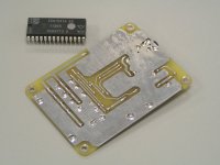
DIR9001+protocol converter module for TDA1541A
Here is a picture of a completed DIR9001 S/PDIF receiver & protocol converter module. It can directly drive a TDA1541A through the simultaneous interface. It is basically a combination of the Toslink receiver plus protocol converter schematics I posted.
This is perhaps the easiest and cleanest way to drive a TDA1541A in simultaneous mode as the discrete low power logic produces very little interference compared to a CPU, ASIC or FPGA. It also supports battery powered operation for a very clean off-line power source.
TDA1541A is added in order to get an impression of the module size.
It is powered by a 3V4 ... 5V external (battery) power supply. On board ultra low noise LP5907-3V3 LDO regulator.
Idling, 13mA, 42.9mW
Streaming 44.1, 15mA, 49.5mW
Streaming 48, 16mA, 49.5mW
Streaming 88.2, 22mA, 72.6mW
Streaming 96, 23mA, 75.9mW
LED lock indicator.
Power supply and LED can be connected to the 4 solder pads on the side of the PCB
3.5mm Toslink input, 44.1, 48, 88.2, 96 KHz.
The DIR9001 is set as follows:
Clock source: PLL.
Format: 24 Bits, Left Justified.
SCK frequency, 256 fs.
Digital interface Output signals:
DOL (Data Out Left channel) for TDA1541A.
DOR (Data Out Right channel) for TDA1541A.
BCKO (Bit Clock Output).
NBCKO (Inverted Bit Clock Output for TDA1541A).
NWIN (Inverted Window signal).
WIN (Non Inverted Window signal).
LEO (Latch Enable Output for TDA1541A).
The extra output signals may come in handy when interfacing to DAC chips other than the TDA1541A.
Attachments
Hi -EC-,
Heroic work, as usual.
Talking about thermal memory distortion, when one realizes its effect there is no way back...
Readings:
La distorsion thermique (Héphaïtos)
Memory Distortion Philosophies
There is a patent also but too heavy to post.
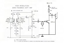
Here I attach the modified diffamp which I pasted into a single ended class A SET amp. Believe me, the improvement in musical bliss is significant.
This one is not simulated. In other unit with BJTs I reached lower THD with the two braches of the input CFP charing equal current by trimming S-E resistors. Now I will further modify it by adding cascoded current sourse and cascoded loads, but that needs time and extensive listening test.
So extensive use of cascodying and CFP makes better amplifying devices but this is advanced art and difficult to tame...for an eternal beginner like yours truly...
Best wishes,
M-
Heroic work, as usual.
Talking about thermal memory distortion, when one realizes its effect there is no way back...
Readings:
La distorsion thermique (Héphaïtos)
Memory Distortion Philosophies
There is a patent also but too heavy to post.
Here I attach the modified diffamp which I pasted into a single ended class A SET amp. Believe me, the improvement in musical bliss is significant.
This one is not simulated. In other unit with BJTs I reached lower THD with the two braches of the input CFP charing equal current by trimming S-E resistors. Now I will further modify it by adding cascoded current sourse and cascoded loads, but that needs time and extensive listening test.
So extensive use of cascodying and CFP makes better amplifying devices but this is advanced art and difficult to tame...for an eternal beginner like yours truly...
Best wishes,
M-
Attachments
I´m leaning away from diff pairs because of the harmonic distribution. It kills the second harmonic which can be sonic gold.
Katz's Corner Episode 25: Adventures in Distortion | InnerFidelity
About thermal distortion, I read parts of the article in french. They mostly tested BJTs with their methodology but it ends with two fets. The 2SK30A did remarkably well, in their words. "Practically no thermal distortion".
I didn´t find the details about the circuit used for the test, bias conditions, etc... But I imagine the fets will exhibit very low thermal effects when operated near the zero tempco. For example, it is around 8mA for the 2sk170 iirc.
As for that circuit idea I recently posted, a very simple one jfet I/V for those that use digital volume, I don´t think there is any concern with thermal effects. Since there is no other bias than the TDA1541 current itself, there can be no bias variations - drain current is exactly the TDA1541 current. I think it´ll work well with the 1541. I already use it with 1543 with excellent results. These dacs have in common the principle: the whole full scale current always flows, but part of it flows outside the chip. In papers, the philips engineers call the current that flows inside the chip "Idump". The sum of Idump and Iout is a constant. That´s why routing Iout to the V+ yields a nearly constant current operation (minus capacitive spikes).
Thanks,
Alex
I´m leaning away from diff pairs because of the harmonic distribution. It kills the second harmonic which can be sonic gold.
Katz's Corner Episode 25: Adventures in Distortion | InnerFidelity
About thermal distortion, I read parts of the article in french. They mostly tested BJTs with their methodology but it ends with two fets. The 2SK30A did remarkably well, in their words. "Practically no thermal distortion".
I didn´t find the details about the circuit used for the test, bias conditions, etc... But I imagine the fets will exhibit very low thermal effects when operated near the zero tempco. For example, it is around 8mA for the 2sk170 iirc.
As for that circuit idea I recently posted, a very simple one jfet I/V for those that use digital volume, I don´t think there is any concern with thermal effects. Since there is no other bias than the TDA1541 current itself, there can be no bias variations - drain current is exactly the TDA1541 current. I think it´ll work well with the 1541. I already use it with 1543 with excellent results. These dacs have in common the principle: the whole full scale current always flows, but part of it flows outside the chip. In papers, the philips engineers call the current that flows inside the chip "Idump". The sum of Idump and Iout is a constant. That´s why routing Iout to the V+ yields a nearly constant current operation (minus capacitive spikes).
Thanks,
Alex
Hi Alexandre,
I was talking amplification in general. Your circuit may be classified as a common-gate buffer (?) , then shall be low distortion, IF power is near constant. As Peufeu stated, constant power is the aim for achieving low TMD.
My modified diffamp is good for example as output differential amplifier for a balanced output DAC, instead of monolythic opamps.
When we investigate for TMD really we are dealing with an entirely different paradigm: just focus on the lowest THD and the most stable circuit possible, the low TMD will do the rest. We are not talking about warmer vs sterile or other comparisons like that; I believe TMD affects more the time frame and not the amplitude frame. It is like an "analog jitter" so to speak. The energy content of the musical phrase is packed more compactly (like in real life) so musical attacks (plucked instruments, string attacks, piano attacks) for example are more pronounced and harmonic content (especially bass harmonics; the bodies of the instruments are more pronounced) from the musical instruments are better conveyed, with a better sound envelope, resulting in a fresher and more natural musical portrait, a more natural breath to the music flow.
And this difference is not one one struggles for to hear: it is instantly recognized by the hearing system as it is the natural way our brain is used to...
For example, I am a violin lover and I usually don't care for guitar...now I am listening more and more guitar with my Amnesis amp, that good it sounds...and it can also clearly show differences in timbres of two guitars for a duo.
Sorry for slight OT...well not completely OT since I am sure -EC- can design a low TMD active output for his DAC.
Cheers,
M.
Your circuit may be classified as a common-gate buffer (?) , then shall be low distortion, IF power is near constant.
Yes, common gate, but I wouldn´t call it my circuit, it is just a very simple and sensible way to convert current to voltage, with the bonus of a constant current draw for the whole DAC circuit because we´re routing Iout to the V+. I think this was overlooked up to now. I´m pretty certain it will be beneficial in terms of these little imperfections that John points out (interferences between digital inputs and analog out), and more.
Because of its simplicity it´s not subject to thermal distortion. Regardless of power. There is no bias current for it to have a "memory effect" from previous values. All distortion will be coming from the tda1541 itself, because of non zero input impedance. The circuit forces Idrain=Iout, there is virtually zero gate current (the few pF of capacitance will only affect components way up at hundreds of KHz).
Nice to hear about your amnesis amp. About the modified diffamp, is the distortion low enough to not matter?
What I was pointing is that dominant third harmonic is not very desirable, unlike dominant second. At least for me. And that guy Bob Katz. He´s a very respected mastering engineer. Good read there.
Thanks and keep up the good work M
-Alex
About the modified diffamp, is the distortion low enough to not matter?
Thanks and keep up the good work M
-Alex
Thanks!
To tell the truth I did not measure nor simulate it
To busy with the Amnesis now...
TDA1541A Dual Mono 17 bit Signed Magnitude DAC
With conventional (R2R / multibit) D/A converters all bits flip over simultaneously at the signal zero crossing. This produces both, switching noise and bit errors.
Our auditory system seems to be highly sensitive to everything that happens around these zero crossings. Now you know why class A amplifiers make a lot of sense as these will reduce but never fix problems around zero crossings and why SE amplifiers -can- sound so musical and involving as these reproduce zero crossings so accurately like no other amp can. The speakers are no exception either, problems, problems.
But lets concentrate on the DAC first. What could cause problems around zero crossings? all bits flipping over at the same time, just at most critical point in the audio signal.
1000000000000000 -> 0111111111111111, we have 16 bits flipping over simultaneously around the zero crossing!
This problem can be fixed if we use a signed magnitude DAC. As the name implies we have a sign bit (positive or negative) indicating the polarity and magnitude information (number) that, well determines the signal magnitude.
And what's so different about this approach?
With signed magnitude we usually have two identical DACs. One handles the positive signal halve only, the other handles the negative signal half only.
Now we can step away from the zero crossing with small steps in both directions like this:
Signal rises from zero crossing to plus, 000000000000000 -> 000000000000001 -> 000000000000010 and so on. L channel never goes below 000000000000000, we have only one bit flipping around the signal crossover, positive DAC is working, negative DAC takes a break.
Signal drops from zero crossing to minus, 111111111111111 -> 111111111111110 -> 111111111111101 and so on. R channel never goes above 111111111111111, we have only one bit flipping around the signal crossover. negative DAC is working, positive DAC takes a break.
MSB now becomes the sign bit that controls the polarity and no longer shows up in the data (magnitude) of both DACs. So we have a spare (extra) bit where MSB used to be. Now we can also double the resolution.
The outputs of both DACs are connected together.
Some examples of signed magnitude D/A converters are the Soekris DAC and the PCM1704 just to name a few of many.
The TDA1541A has two identical DACs that are usually used for L and R channel. But what if we used both channels to construct a signed magnitude mono DAC with it? We would need two TDA1541A chips as we need 4 DACs in total now. We end up with a 17 bit dual mono TDA1541A signed magnitude DAC, full scale current doubles to 8mA and resolution is doubled to 17 bits. Now this would be a very nice project for two (double crown) TDA1541A chips.
All we need to do is design a decoder that moves some bits around so we end up with output signals DOL- and DOL+ for TDA1541A #1 and DOR- and DOR+ for TDA1541A #2.
We could use a FPGA or ASIC, however, the nasty thing here is that we need to reduce (switching) noise to lowest practical level and that's going to be extremely difficult with these LSI chips that produce very strong interference. Even a tiny PAL (Programmable Array Logic) produces massive switching noise and draws a lot of current.
So there is little other option then building a decoder from a handful of discrete logic so we only use and connect those logic building blocks we need and we can locally decouple all these logic building blocks until switching noise is as low as it gets. Current consumption is also absolute minimum this way.
IF we insist using a noisy ASIC or CPU we have to ensure that the D/A converter is -completely- shielded (EMI included) from this switching noise, I wish you good luck with that.
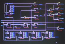
Back to the Decoder circuit. I attached a schematic of a decoder I designed for this experiment, it is based on the protocol converter I posted earlier. It looks complicated but it is basically as simple as it gets.
We need to do a few things, sample and hold the MSBs, then loose the LSBs from the serial data that goes into the TDA1541A chips. Mix MSB and data signals together so we get dedicated data signals for each TDA1541A.
We know that the MSB are located immediately after a WS change (I use Left justified format!). So we need to create a trigger signal right at the center of these MSBs. We need 0.5 bit delay for that and that's provided by U1. We need to keep the Left MSB with the Left data and the Right MSB with the right data. So we have to invert the 0.5 bit delay signal for one channel. U4 and U5 sample and hold the MSB for each channel, we use these sampled MSBs in the decoder stage.
Loose the MSB, easier said then done as we can't easily shift the serial data to the left unless we add some more shift registers.
Instead I delayed the window that determines when the output signals are generated in relation to WS. By delaying the window signal by one bit I basically removed the MSBs from the serial bit stream, after I have sampled the MSBs of course.
The output of U2 provides a 1 bit delay and the delayed signal goes to the window generator built around counter U6 and NOR gate U17.
U3 lines up the left channel data so the bits are valid on the falling edge of BCKI (TDA1541A clocks on the falling edge of BCK when configured in the simultaneous mode).
U7 ... U10 line up the Right channel data with the Left channel data so both can be clocked out simultaneously.
U16 gates the bit clock so we have a 16 bit clock burst at just the right time. The window signal enables and disables the continuous BCKI signal.
U13 B and D do the same for the serial data, creating 16 bit data bursts at just the right moment.
U13A, U14, U13C and U15 form a simple AND / OR decoder that extracts DOL-, DOL+, DOR-, and DOR+ signals from the serial data streams.
People who need to have I2S input will have to add some more logic as MSB is shifted one bit to the right (with respect to WS) and both channels are swapped.
What we have to do now is adding one extra D flip-flops to sample the MSBs one and a half bit after a WS change (1.5 bit delay) and a 2 bit delay to drive the window generator so we still loose the MSB. DOL becomes DOR and DOR becomes DOL (swap channels) and we are ready to use I2S input signal.
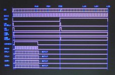
Second picture shows the timing diagram. We can see that the whole window is shifted one bit to the right compared to the protocol converter timing diagram.
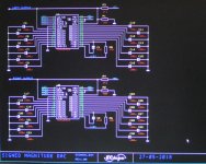
Third schematic shows the TDA1541A section. We need +4mA bias current for biasing two converters. This can be done using a 1K1 resistor between outputs and +5V. I try to avoid a CCS whenever possible as these are -very- nasty circuits that often result in grainy fatiguing sound. I traced this back to the non-linear impedance that varies with frequency, adding a shunt resistor across the CCS can improve things a bit by linearising the impedance.
The simple CCS we see in many schematics are not very precise and for this application we need a high precision CCS with very large bandwidth and superb impedance linearity. This usually translates to complex analogue circuits that in turn introduce new problems.
The full scale current has doubled to 8mA so the passive I/V resistor value has to be reduced to 75 Ohms. We get approx. 560mVpp output (1K1 is in parallel with 75R for ac). This lower output impedance comes in handy when we like to drive a step up transformer or a TVC with a gain tap.
With conventional (R2R / multibit) D/A converters all bits flip over simultaneously at the signal zero crossing. This produces both, switching noise and bit errors.
Our auditory system seems to be highly sensitive to everything that happens around these zero crossings. Now you know why class A amplifiers make a lot of sense as these will reduce but never fix problems around zero crossings and why SE amplifiers -can- sound so musical and involving as these reproduce zero crossings so accurately like no other amp can. The speakers are no exception either, problems, problems.
But lets concentrate on the DAC first. What could cause problems around zero crossings? all bits flipping over at the same time, just at most critical point in the audio signal.
1000000000000000 -> 0111111111111111, we have 16 bits flipping over simultaneously around the zero crossing!
This problem can be fixed if we use a signed magnitude DAC. As the name implies we have a sign bit (positive or negative) indicating the polarity and magnitude information (number) that, well determines the signal magnitude.
And what's so different about this approach?
With signed magnitude we usually have two identical DACs. One handles the positive signal halve only, the other handles the negative signal half only.
Now we can step away from the zero crossing with small steps in both directions like this:
Signal rises from zero crossing to plus, 000000000000000 -> 000000000000001 -> 000000000000010 and so on. L channel never goes below 000000000000000, we have only one bit flipping around the signal crossover, positive DAC is working, negative DAC takes a break.
Signal drops from zero crossing to minus, 111111111111111 -> 111111111111110 -> 111111111111101 and so on. R channel never goes above 111111111111111, we have only one bit flipping around the signal crossover. negative DAC is working, positive DAC takes a break.
MSB now becomes the sign bit that controls the polarity and no longer shows up in the data (magnitude) of both DACs. So we have a spare (extra) bit where MSB used to be. Now we can also double the resolution.
The outputs of both DACs are connected together.
Some examples of signed magnitude D/A converters are the Soekris DAC and the PCM1704 just to name a few of many.
The TDA1541A has two identical DACs that are usually used for L and R channel. But what if we used both channels to construct a signed magnitude mono DAC with it? We would need two TDA1541A chips as we need 4 DACs in total now. We end up with a 17 bit dual mono TDA1541A signed magnitude DAC, full scale current doubles to 8mA and resolution is doubled to 17 bits. Now this would be a very nice project for two (double crown) TDA1541A chips.
All we need to do is design a decoder that moves some bits around so we end up with output signals DOL- and DOL+ for TDA1541A #1 and DOR- and DOR+ for TDA1541A #2.
We could use a FPGA or ASIC, however, the nasty thing here is that we need to reduce (switching) noise to lowest practical level and that's going to be extremely difficult with these LSI chips that produce very strong interference. Even a tiny PAL (Programmable Array Logic) produces massive switching noise and draws a lot of current.
So there is little other option then building a decoder from a handful of discrete logic so we only use and connect those logic building blocks we need and we can locally decouple all these logic building blocks until switching noise is as low as it gets. Current consumption is also absolute minimum this way.
IF we insist using a noisy ASIC or CPU we have to ensure that the D/A converter is -completely- shielded (EMI included) from this switching noise, I wish you good luck with that.
Back to the Decoder circuit. I attached a schematic of a decoder I designed for this experiment, it is based on the protocol converter I posted earlier. It looks complicated but it is basically as simple as it gets.
We need to do a few things, sample and hold the MSBs, then loose the LSBs from the serial data that goes into the TDA1541A chips. Mix MSB and data signals together so we get dedicated data signals for each TDA1541A.
We know that the MSB are located immediately after a WS change (I use Left justified format!). So we need to create a trigger signal right at the center of these MSBs. We need 0.5 bit delay for that and that's provided by U1. We need to keep the Left MSB with the Left data and the Right MSB with the right data. So we have to invert the 0.5 bit delay signal for one channel. U4 and U5 sample and hold the MSB for each channel, we use these sampled MSBs in the decoder stage.
Loose the MSB, easier said then done as we can't easily shift the serial data to the left unless we add some more shift registers.
Instead I delayed the window that determines when the output signals are generated in relation to WS. By delaying the window signal by one bit I basically removed the MSBs from the serial bit stream, after I have sampled the MSBs of course.
The output of U2 provides a 1 bit delay and the delayed signal goes to the window generator built around counter U6 and NOR gate U17.
U3 lines up the left channel data so the bits are valid on the falling edge of BCKI (TDA1541A clocks on the falling edge of BCK when configured in the simultaneous mode).
U7 ... U10 line up the Right channel data with the Left channel data so both can be clocked out simultaneously.
U16 gates the bit clock so we have a 16 bit clock burst at just the right time. The window signal enables and disables the continuous BCKI signal.
U13 B and D do the same for the serial data, creating 16 bit data bursts at just the right moment.
U13A, U14, U13C and U15 form a simple AND / OR decoder that extracts DOL-, DOL+, DOR-, and DOR+ signals from the serial data streams.
People who need to have I2S input will have to add some more logic as MSB is shifted one bit to the right (with respect to WS) and both channels are swapped.
What we have to do now is adding one extra D flip-flops to sample the MSBs one and a half bit after a WS change (1.5 bit delay) and a 2 bit delay to drive the window generator so we still loose the MSB. DOL becomes DOR and DOR becomes DOL (swap channels) and we are ready to use I2S input signal.
Second picture shows the timing diagram. We can see that the whole window is shifted one bit to the right compared to the protocol converter timing diagram.
Third schematic shows the TDA1541A section. We need +4mA bias current for biasing two converters. This can be done using a 1K1 resistor between outputs and +5V. I try to avoid a CCS whenever possible as these are -very- nasty circuits that often result in grainy fatiguing sound. I traced this back to the non-linear impedance that varies with frequency, adding a shunt resistor across the CCS can improve things a bit by linearising the impedance.
The simple CCS we see in many schematics are not very precise and for this application we need a high precision CCS with very large bandwidth and superb impedance linearity. This usually translates to complex analogue circuits that in turn introduce new problems.
The full scale current has doubled to 8mA so the passive I/V resistor value has to be reduced to 75 Ohms. We get approx. 560mVpp output (1K1 is in parallel with 75R for ac). This lower output impedance comes in handy when we like to drive a step up transformer or a TVC with a gain tap.
Attachments
Tda1545 and Tda1387 use this same technique. Philips calls it symmetrical offset decoding.
If you read Philips papers you learn that implementing a fairly accurate 10 bit DAC is easy. This is done in a simple way such as a "passive 10-bit current divider based on emitter scaling". This is how they describe it for the Tda1541, but it is similar on the cmos dacs. This 10-bit "easy" dac is what they use for the LSBs.
The hard stuff is actually the 11th bit up to the MSB. That´s where they used DEM (in the Tda1541) and CC (continous calibration, in the cmos dacs).
The choice of doing "symmetrical offset decoding" with the Tda1541 looks like a very good one to me. It looks like an excellent solution, we have two "easy" 10-bit dacs (above and below zero), and the DEM stuff (which is more subject to glitches/innacuracies) only happens away from zero. Where our hearing is less sensitive to these problems.
Thanks,
Alex
CC-DACs use symmetrical offset decoding in which the bit switching is arranged so that the zero-crossing transition is performed by switching only the smallest currents. The intrinsic highly accurate coarse current, combined with the symmetrical offset principle, precludes any distortion at the zero-crossing or at any other small-signal transitions. CC-DACs are therefore capable of high-quality reproduction of low-level audio input signals.
If you read Philips papers you learn that implementing a fairly accurate 10 bit DAC is easy. This is done in a simple way such as a "passive 10-bit current divider based on emitter scaling". This is how they describe it for the Tda1541, but it is similar on the cmos dacs. This 10-bit "easy" dac is what they use for the LSBs.
The hard stuff is actually the 11th bit up to the MSB. That´s where they used DEM (in the Tda1541) and CC (continous calibration, in the cmos dacs).
The choice of doing "symmetrical offset decoding" with the Tda1541 looks like a very good one to me. It looks like an excellent solution, we have two "easy" 10-bit dacs (above and below zero), and the DEM stuff (which is more subject to glitches/innacuracies) only happens away from zero. Where our hearing is less sensitive to these problems.
Thanks,
Alex
- Home
- Source & Line
- Digital Line Level
- Building the ultimate NOS DAC using TDA1541A