Hi tessier,
Here are some basic properties for a TDA1541A I/V stage :
- Output compliance of +25 / -25mV at the DAC output -must- be met, these are absolute maximum values.
- Bandwidth of the TDA1541A output signal must be limited prior to feeding it into an I/V stage.
- All bit currents -must- be returned to +5V
- The I/V stage should be perfectly able to handle the presented bandwidth.
- Full DC-coupling is -required-
- I/V stage should be able to resolve signals down to 61 nano amperes / 30 microvolts.
Your circuit generates -0.004 * 35 = -140mV at the DAC output, this grossly exceeds output compliance. Since no +2mA bias current is used, signal does not swing around 0V, this increases the problem.
When using a suitable +2mA bias current source, max. I/V resistor value would be: 0.05 / 0.004 = 12.5 Ohms. If the +2mA bias current is not used, the I/V resistor value has to be reduced to 6.25 Ohms.
The bandwidth of the TDA1541A output signal is too large to directly drive a passive I/V resistor or circuit. So the output signal must be bandlimited prior to feeding it to an I/V resistor or active circuit. This can be done by connecting a suitable capacitor between TDA1541A output and GND or connecting a suitable capacitor at the output of a step-up transformer.
Step up transformers can limit bandwidth, provide sufficient signal amplitude while meeting output compliance, and also handle low level signals quite well.
Suppose we use a Sowther 9762 1:12.8 step-up transformer. When using a 1K I/V resistor at the transformer secondary, the reflected secondary load will be 1000 / 12.8^2 = 6.1 Ohm. This will meet output compliance (-0.004 * 6.1 = -24.4mV). The output signal amplitude will then be 312mVpp. If an output signal of say 6.65V is required, tube amplifier gain needs to be 18.
It is also possible to use both secondary windings of the 9762 to drive a differential tube amplifier stage. In this case we have 2 I/V resistors of 500 Ohms each.
This however doesn't solve the issue with bit return currents. The selected bit currents are routed through the reflected load of 6.1 Ohm to GND. The unselected bit currents are routed to +5V (inside the TDA1541A). This means that the load current on the +5V varies with the signal, this results in a ripple voltage that is extremely difficult to reduce to required low levels in the microvolt range. The ripple on the +5V (that also powers logic circuits) will introduce trigger uncertainty, introducing deterministic jitter (jitter related to music content).
The use of a transformer no longer provides full DC-coupling, full DC-coupling is required for highest transparency.
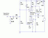
How about this ECC82 IV amp buffer for the tda1541a ?
Here are some basic properties for a TDA1541A I/V stage :
- Output compliance of +25 / -25mV at the DAC output -must- be met, these are absolute maximum values.
- Bandwidth of the TDA1541A output signal must be limited prior to feeding it into an I/V stage.
- All bit currents -must- be returned to +5V
- The I/V stage should be perfectly able to handle the presented bandwidth.
- Full DC-coupling is -required-
- I/V stage should be able to resolve signals down to 61 nano amperes / 30 microvolts.
Your circuit generates -0.004 * 35 = -140mV at the DAC output, this grossly exceeds output compliance. Since no +2mA bias current is used, signal does not swing around 0V, this increases the problem.
When using a suitable +2mA bias current source, max. I/V resistor value would be: 0.05 / 0.004 = 12.5 Ohms. If the +2mA bias current is not used, the I/V resistor value has to be reduced to 6.25 Ohms.
The bandwidth of the TDA1541A output signal is too large to directly drive a passive I/V resistor or circuit. So the output signal must be bandlimited prior to feeding it to an I/V resistor or active circuit. This can be done by connecting a suitable capacitor between TDA1541A output and GND or connecting a suitable capacitor at the output of a step-up transformer.
Step up transformers can limit bandwidth, provide sufficient signal amplitude while meeting output compliance, and also handle low level signals quite well.
Suppose we use a Sowther 9762 1:12.8 step-up transformer. When using a 1K I/V resistor at the transformer secondary, the reflected secondary load will be 1000 / 12.8^2 = 6.1 Ohm. This will meet output compliance (-0.004 * 6.1 = -24.4mV). The output signal amplitude will then be 312mVpp. If an output signal of say 6.65V is required, tube amplifier gain needs to be 18.
It is also possible to use both secondary windings of the 9762 to drive a differential tube amplifier stage. In this case we have 2 I/V resistors of 500 Ohms each.
This however doesn't solve the issue with bit return currents. The selected bit currents are routed through the reflected load of 6.1 Ohm to GND. The unselected bit currents are routed to +5V (inside the TDA1541A). This means that the load current on the +5V varies with the signal, this results in a ripple voltage that is extremely difficult to reduce to required low levels in the microvolt range. The ripple on the +5V (that also powers logic circuits) will introduce trigger uncertainty, introducing deterministic jitter (jitter related to music content).
The use of a transformer no longer provides full DC-coupling, full DC-coupling is required for highest transparency.
Hi tessier,
This however doesn't solve the issue with bit return currents. The selected bit currents are routed through the reflected load of 6.1 Ohm to GND. The unselected bit currents are routed to +5V (inside the TDA1541A). This means that the load current on the +5V varies with the signal, this results in a ripple voltage that is extremely difficult to reduce to required low levels in the microvolt range. The ripple on the +5V (that also powers logic circuits) will introduce trigger uncertainty, introducing deterministic jitter (jitter related to music content).
The use of a transformer no longer provides full DC-coupling, full DC-coupling is required for highest transparency.
So are you saying that the only sufficient I/V stage for a TDA1541 is power by the same +5V for the chip? That would severely limit any potential I/V stage design. This just doesn't sound reasonable, basically our only option would be an IC opamp or a terribly high distorting jfet buffer.
Hi tessier,
This however doesn't solve the issue with bit return currents. The selected bit currents are routed through the reflected load of 6.1 Ohm to GND. The unselected bit currents are routed to +5V (inside the TDA1541A). This means that the load current on the +5V varies with the signal, this results in a ripple voltage that is extremely difficult to reduce to required low levels in the microvolt range. The ripple on the +5V (that also powers logic circuits) will introduce trigger uncertainty, introducing deterministic jitter (jitter related to music content).
QUOTE]
Hello John,
could You please explain how the issue with bit return currents is solved in the MK14 I/V circuit shown in post #4489?
Thank You for your support
Hi tessier,
Here are some basic properties for a TDA1541A I/V stage :
- Output compliance of +25 / -25mV at the DAC output -must- be met, these are absolute maximum values.
- Bandwidth of the TDA1541A output signal must be limited prior to feeding it into an I/V stage.
- All bit currents -must- be returned to +5V
- The I/V stage should be perfectly able to handle the presented bandwidth.
- Full DC-coupling is -required-
- I/V stage should be able to resolve signals down to 61 nano amperes / 30 microvolts...
Hi
I've seen in the thread that some guy's suggested to use the Aikido tube preamp as a IV amp.
Is it a good ideas and could you tell me where I can find a IV amp circuit using the Aikido ?
I have few 12AU7 to made a IV amp.
Thanx a lot.
Paul
Last edited:
So are you saying that the only sufficient I/V stage for a TDA1541 is power by the same +5V for the chip? That would severely limit any potential I/V stage design. This just doesn't sound reasonable, basically our only option would be an IC opamp or a terribly high distorting jfet buffer.
Check the datasheet of the TDA1542 and how the opamps are powered...
ECC82 is good in general for amplifying the low signal after the R-IV.
iF You dont mind the higher output resistance of 6K cca. caused with 6.5K-7K Internal resistance of the tube? In a simple basic topology.
And phases will be good too because R-iv shifts of 180deg and Tube stage shifts too of 180 deg...
But this circuit from post 4701 is complicated, no additional phase shift,
tooo many C on signal path, AND very low anode voltages 40V cca per tube section...
Tis is tube deserves higher voltage, not a transistor.
there is no need for that, but just for plain circuit.
cheers
Q for EC
will the low values of R-IV like 6 to 12 ohms overheat the TDA1541A chip
from Your knowledge?
I think with an I/V resistor this low the only chance would be a Jfet phopreamp type gain stage.
With a tube the SNR would kill resolution.
One of the quietest tubes is a triode strapped D3A and it has nice gain but even it would have trouble amplifiying a .002mAx10 ohms*0.0015849 LSB = 0.03 micro Volt signal.
Probably end up with a 12 bit resolution DAC at best with a 10 ohm I/V resistor.
Oleg did some measurements and found that a 33 ohm resistor with the 2mA offset handled as Pedra does was the best compromise for a tube gain.
Hi JOSI,
Here the selected bit currents are not returned to +5V, this is one of the reasons why I no longer use this I/V circuit.
could You please explain how the issue with bit return currents is solved in the MK14 I/V circuit shown in post #4489?
Here the selected bit currents are not returned to +5V, this is one of the reasons why I no longer use this I/V circuit.
Hi tessier,
Here you can find information about Aikiodo amplifiers and kits:
GlassWare Line Stage & Headphone Amplifiers Kits and PCBs
Aikido LV
Is it a good ideas and could you tell me where I can find a IV amp circuit using the Aikido ?
Here you can find information about Aikiodo amplifiers and kits:
GlassWare Line Stage & Headphone Amplifiers Kits and PCBs
Aikido LV
No need to disturb EC for this one - no, the TDA1541A is current-out so even shorting its output will do no damage at all.
Hm...Did You tried to short Iout to gnd?

I tried it. The chip delivers constant current into a short circuit. However I noticed that the chip is rather hot (even during normal load, not just with shorted output). So I glued a copper heatsink on top in order to reduce the surface temperature, reduce vibration (might be woodoo, but costs nothing), and reduce EMC sensitivity. I grounded the heatsink with a piece of wire to DGND.
Hi Zoran,
TDA1541A is based on current mode logic / transistors, CML draws a constant current, this is why the TDA1541A gets hot. The advantage of CML is that supply current remains the same during switching or during steady state. This results in low on-chip switching noise.
Modern DAC chips are based on CMOS logic, CMOS logic only draws current during switching as stray capacitance needs to be charged / discharged. These chips run much cooler, but the large differences in supply current between steady state and swithing leads to high on-chip switching noise.
TDA1541A Typical power dissipation: 700mW
TDA1541A Maximum power dissipation 1W
Power dissipation doesn't change with load impedance.
The same as without load, in free air @ 19 dedrees Celcius room temperature, chip surface temperature (center of the chip) is around 40 degrees Celcius (typical). Chip temperature can rise significantly when the chip is placed in a closed housing without sufficient (convection) cooling and elevated ambient temperature inside that housing.
but what about heating of the chip?
TDA1541A is based on current mode logic / transistors, CML draws a constant current, this is why the TDA1541A gets hot. The advantage of CML is that supply current remains the same during switching or during steady state. This results in low on-chip switching noise.
Modern DAC chips are based on CMOS logic, CMOS logic only draws current during switching as stray capacitance needs to be charged / discharged. These chips run much cooler, but the large differences in supply current between steady state and swithing leads to high on-chip switching noise.
TDA1541A Typical power dissipation: 700mW
TDA1541A Maximum power dissipation 1W
Power dissipation doesn't change with load impedance.
what is the temperature of the chip with very low, Riv?
The same as without load, in free air @ 19 dedrees Celcius room temperature, chip surface temperature (center of the chip) is around 40 degrees Celcius (typical). Chip temperature can rise significantly when the chip is placed in a closed housing without sufficient (convection) cooling and elevated ambient temperature inside that housing.
Hi JOSI,
Here the selected bit currents are not returned to +5V, this is one of the reasons why I no longer use this I/V circuit.
would it be possible to post your last MK18 principle schema?
Hi ryanj,
BF862 has yfs of 45 (typical) and Ft of 715 MHz. So we have both, high gain and high limiting frequency. That's why I chose this specific JFET for this application.
The input impedance of a grounded-gate circuit equals approx. 1 / gm. So current buffer input impedance equals approx. 1 / 0.045 = 22 Ohms. With 4mA full-scale current, max. ac voltage amplitude on TDA1541A current output equals 0.004 * 22 = 88mV or +/- 44mV.
1.94Vpp with 500R passive I/V resistor and PCS impedance of 16,400 Ohms.
It is actually a Passive Current Source based on a stabilised voltage and a series resistor. Thermal drift is very low (combination of both, power supply and resistor thermal drift). Thermal drift is much lower compared to a CCS.
The higher the series resistor value (impedance) the more the PCS resembles an ideal CCS.
The problem is that when using relatively low voltage and relatively high series resistor value, the target current may not be obtained (too low). By increasing the supply voltage target current can be obtained and impedance can be increased.
Example:
3mA target current, 20V supply and 1V DC across the load would require 19 / 0.003 = 6K333 resistor. So the PCS impedance would now be 6K333.
3mA target current, 200V supply and 1V DC across the load would require 199 / 0.003 = 66K333. Now the PCS impedance is raised to 66K333 while maintaining target output current of 3mA.
Advantages of a PCS:
- Constant impedance over very large frequency range (use of RF resistors extends range).
- Instant response, no feedback loops, no delays.
- Very low distortion.
- Very low thermal drift.
- Very low noise.
I attached MK14 I/V circuit schematics.
T10 and T11 form a cascode current buffer. P1 sets DC voltage at DAC output at 0V DC. Bandwidth approximates JFET Ft (715 MHz).
R4 sets negative bias current of -15 / 5600 = -2.7mA. PCS impedance equals 5600 Ohms and is in parallel with 22 Ohm cascode current buffer input impedance.
R1 and R2 set positive supply current of +7mA, PCS impedance equals 16,400 Ohms and is in parallel with 500 Ohm passive I/V resistor so actual I/V resistor value is reduced to 485 Ohms.
The cascode current buffer output current is fed to the 500 Ohm passive I/V resistor that connects to GND.
Current / voltage swing:
DAC output current = 0mA (minimum current), I/V resistor current equals +7mA - 2.7mA = +4.3mA, voltage across I/V resistor equals +2.0855V
DAC output current = 2mA (bias current - no signal), I/V resistor current equals +7mA - 2mA - 2.7mA = +2.3mA, voltage across I/V resistor equals +1.1155V
DAC output current = 4mA (full-scale), I/V resistor current equals +7mA - 4mA - 2.7mA = +0.3mA, voltage across I/V resistor equals +0.1455V
The +115V supply now enables higher output amplitude.
Example:
10K passive I/V resistor. DC voltage (2mA bias) equals 20V. PCS series resistor equals (115-20) / 0.007 =13K57. This resistor is in parallel with 10K so I/V resistor value drops to 5.76K
Output amplitude now equals 0.004 * 5760 = 23.4Vpp.
This opens the possibility of using a unity gain bridge buffer (Circlotron) instead of a conventional amplifier to drive the speakers. With 23Vpp on each bridge half we would get approx. 16V rms. This would give approx. 32 watts rms in 8 Ohms.
When using 2 x TDA1541A (phase / anti-phase outputs) it would only take two power MOSFETs and a power supply to drive the speaker.
Can this be applied to the TDA1543?
what would be the bias currents? Possible to avoid the -15V rail?
Last edited:
guido please could You point the link for TDA1542
I try to find, but without success
thanks
Here is.
Attachments
- Home
- Source & Line
- Digital Line Level
- Building the ultimate NOS DAC using TDA1541A