Hi, wlowes
This is useful with standpoint of the improvement to insulation, but can enlarge the stray montage capacities.
I think that at given aspect it is more important to pay attention to DEM capacitor insulation.
It is necessary to choose the capacitors with maximum resistance of the insulation, let in the prejudice of the other parameter even.
Would it not be better to use a pcb that has most of the chip floating in the air?
This is useful with standpoint of the improvement to insulation, but can enlarge the stray montage capacities.
I think that at given aspect it is more important to pay attention to DEM capacitor insulation.
It is necessary to choose the capacitors with maximum resistance of the insulation, let in the prejudice of the other parameter even.
Hi, qusp
It is important for correct working of DEM cells low capacitor leakage of at DC. But you talk about electromagnetic hindrances, which are connected with AC. Of course, advisable reduce these hindrances. But here talk about the other.
Parasitic leakage will find a way even without a PCB, without a PCB and ground, EMC noise from the i2s and clock signals will have a whale of a time jumping all over the place. depending on speeds they dont even need a conductor to travel on.
It is important for correct working of DEM cells low capacitor leakage of at DC. But you talk about electromagnetic hindrances, which are connected with AC. Of course, advisable reduce these hindrances. But here talk about the other.
Last edited:
no, it is not just connected to AC, it is connected to i2s, a fast analogue signal used to transmit digital, so kinda AC if you want to look at it that way. fast signals without proper layout/grounding = EMC issues. No i'm not talking about 'other' I also wasnt really talking about capacitors, so I really have no idea what you are talking about....
basically, I know what I was saying, either you didnt understand..or you didnt understand.... and about your post...I didnt understand....
basically, I know what I was saying, either you didnt understand..or you didnt understand.... and about your post...I didnt understand....
Last edited:
Hi, qusp
We have not understood each other. I spoke about the DEM capacitor insulation on direct current, but you spoke of electromagnetic hindrances. This is a separate subject.
Let's return towards the insulation quality of the DEM capacitor.Why this it is important? Because leakages of DEM capacitors on direct current (on DC) break the exact double difference of bit currents at nearby bits. This brings appearance of distortion at analog signal.
basically, I know what I was saying, either you didnt understand..or you didnt understand.... and about your post...I didnt understand....
We have not understood each other. I spoke about the DEM capacitor insulation on direct current, but you spoke of electromagnetic hindrances. This is a separate subject.
Let's return towards the insulation quality of the DEM capacitor.Why this it is important? Because leakages of DEM capacitors on direct current (on DC) break the exact double difference of bit currents at nearby bits. This brings appearance of distortion at analog signal.
no, it is not just connected to AC, it is connected to i2s, a fast analogue signal...
Oh, really? I2S, a fast analogue signal? "Contributing" this kind of feedback seems a bit counterproductive. BTW, no guilt saying that.
Just in case you need a bit of background on this new digital stuff, here you go:
http://en.wikipedia.org/wiki/I²S
Last edited:
haha man how childish can you be....
seems you completely misunderstood the post, but that doesnt surprise me
I was replying to wlowes suggestion that by removing the PCB you would lower the leakages and improve the decoupling by reminding that without a low impedance ground/ ground plane, the fast signals would cause other EM related leakages
yeah clock wave is sooo digital isnt it? the interpretation is digital, the wave that represents it is not
I suggest you go back and hit the books while I make you disappear
Last edited:
haha man how childish can you be....
seems you completely misunderstood the post, but that doesnt surprise me
I was replying to wlowes suggestion that by removing the PCB you would lower the leakages and improve the decoupling by reminding that without a low impedance ground plane the fast signals would cause other EM related leakages
yeah clock wave is sooo digital isnt it? the interpretation is digital, the wave that represents it is not
I suggest you go back and hit the books while I make you disappear
Quote (again) what you wrote..."... it is connected to i2s, a fast analogue signal."
Whatever. I guess I'll get back to my childish Grade 2 reading primer to try and wrap my head around sentence structure.
Hi, jameshillj
May suit and ceramic capacitors with good insulation and with enough big working voltage (100V, 250 V and more). The ceramic capacitor inductance is small.
How see, choice of the type capacitor - not open-and-shut case. Here needs the compromise.
Yes, these capacitors have pretty good insulation, but rather greater size and stray inductance too. The bulky capacitors it is difficult to place and they sensitive to external hindrance.Serg,
I assume from this that Styrene, Teflon or Propylene capacitors for the DEM oscilator are recommended, yes?
May suit and ceramic capacitors with good insulation and with enough big working voltage (100V, 250 V and more). The ceramic capacitor inductance is small.
How see, choice of the type capacitor - not open-and-shut case. Here needs the compromise.
haha man how childish can you be....
seems you completely misunderstood the post, but that doesnt surprise me
I was replying to wlowes suggestion that by removing the PCB you would lower the leakages and improve the decoupling by reminding that without a low impedance ground/ ground plane, the fast signals would cause other EM related leakages
yeah clock wave is sooo digital isnt it? the interpretation is digital, the wave that represents it is not
I suggest you go back and hit the books while I make you disappear
Why is it so hard for people to understand that any digital signal transmission is an analog? Its just basic physics.
As far as the PCB-less TDA1541, the concept is you build it point to point in three dimensions on a copper ground plane , Thorsten calls it "bug" building. The results are aesthetically ugly and not commercially viable but make a lot of "sense" on a science/engineering level, perfect for DIY
 This is why you see little innovation/offerings of TDA1541 PCB's other than the silly china offerings, they just don't make a lot of sense any more.
Hi tessier,
DATA and WS attenuators are designed for 3V3 signals (SD8-transport also outputs 3V3 signals).
For WS and DATA:
1K series resistor between digital audio source and TDA1541A I2S input.
680 Ohm pull-down resistor between TDA1541A I2S input and GND.
1K pull up resistor between TDA1541A I2S input and 3V3 (use digital audio source power supply).
Hi,
I was just re-reading...
So for 3.3V application, BCK attenuation stays about the same with 5x 100R resistors, inductor, 220R pull-up, 68R pull down?...
Thanks
Hi crobbins5421,
In the latest projects I use a high speed / low jitter divide-by-4 circuit running on 1.8V (1.8Vpp output signal). I feed this 1.8Vpp BCK signal to the TDA154x using only a 180R series resistor.
Zero BCK jitter doesn't solve the jitter problem because the DAC chip adds considerable jitter of its own (cumulative jitter) this could well be in the range of 50 … 500ps.
In other words, when we use a DAC chip that contributes typical jitter of say 130ps, then jitter cannot drop below this value when using a zero jitter timing signal.
DAC chip jitter contribution can be theoretically reduced or cancelled by means of active jitter control.
So for 3.3V application, BCK attenuation stays about the same with 5x 100R resistors, inductor, 220R pull-up, 68R pull down?…
In the latest projects I use a high speed / low jitter divide-by-4 circuit running on 1.8V (1.8Vpp output signal). I feed this 1.8Vpp BCK signal to the TDA154x using only a 180R series resistor.
Zero BCK jitter doesn't solve the jitter problem because the DAC chip adds considerable jitter of its own (cumulative jitter) this could well be in the range of 50 … 500ps.
In other words, when we use a DAC chip that contributes typical jitter of say 130ps, then jitter cannot drop below this value when using a zero jitter timing signal.
DAC chip jitter contribution can be theoretically reduced or cancelled by means of active jitter control.
Hi crobbins5421,
In the latest projects I use a high speed / low jitter divide-by-4 circuit running on 1.8V (1.8Vpp output signal). I feed this 1.8Vpp BCK signal to the TDA154x using only a 180R series resistor.
Zero BCK jitter doesn't solve the jitter problem because the DAC chip adds considerable jitter of its own (cumulative jitter) this could well be in the range of 50 … 500ps.
In other words, when we use a DAC chip that contributes typical jitter of say 130ps, then jitter cannot drop below this value when using a zero jitter timing signal.
DAC chip jitter contribution can be theoretically reduced or cancelled by means of active jitter control.
Hi John, thanks for sharing.
If I remember correctly, your current setup has been the same for a while (maybe with some excursions into other solutions coming back to 1.8v flipflops and a current limiting resistor).
Is the development of the dac now at the 'ultimate' status, are are you still working on other elements of it?
Promising wordsDAC chip jitter contribution can be theoretically reduced or cancelled by means of active jitter control.
Could you give some more theory behind this concept?Hi s3tup,
Every DAC receives DATA and generates output signals, these introduce clearly audible deterministic jitter.
Every DAC requires some timing signals (MCK, BCK, WS), if the DAC runs on a mains power supply there is 60 … 120 Hz hum, these introduce audible periodic jitter.
Every DAC contains circuits that generate noise, this introduces random jitter that increases the noise floor and masks signals.
So every DAC suffers from all these 3 types of jitter, even if the timing signal(s) would have zero jitter. Needless to say that timing signal jitter would make matters even worse.
The audibility of this jitter spectrum depends on connected audio set resolution. Sets with high resolution will reveal even the slightest degrading caused by very low jitter levels.
The jitter spectrum contributed by each DAC chip is unique, this is why DAC chips with similar specs can still sound totally different. It also means that when DAC jitter contribution could be canceled, all DAC chips with similar specs could sound exactly the same.
Jitter has a spectrum, shape and carrier frequency. Hearability of jitter relies on the phase noise spectra. Thus without knowing the spectral content of added jitter we can't guess we couldn't hear it…
Every DAC receives DATA and generates output signals, these introduce clearly audible deterministic jitter.
Every DAC requires some timing signals (MCK, BCK, WS), if the DAC runs on a mains power supply there is 60 … 120 Hz hum, these introduce audible periodic jitter.
Every DAC contains circuits that generate noise, this introduces random jitter that increases the noise floor and masks signals.
So every DAC suffers from all these 3 types of jitter, even if the timing signal(s) would have zero jitter. Needless to say that timing signal jitter would make matters even worse.
The audibility of this jitter spectrum depends on connected audio set resolution. Sets with high resolution will reveal even the slightest degrading caused by very low jitter levels.
The jitter spectrum contributed by each DAC chip is unique, this is why DAC chips with similar specs can still sound totally different. It also means that when DAC jitter contribution could be canceled, all DAC chips with similar specs could sound exactly the same.
Referring to post #2738 http://www.diyaudio.com/forums/digi...e-nos-dac-using-tda1541a-274.html#post1784706, I would like to know if a lock condition is possible in NOS on 4 x fWS (176.4 kHz). I calculated the internal timing R for the above C values, and it seems that R is around 12.2 kohm. So the C giving 176.4 kHz fDEM might be around 465 pF. Will test it in the coming days...... Like mentioned before, DEM clock oscillator is able to "lock" on (on-chip) BCK crosstalk. By selecting DEM clock capacitor values that produce (almost) exact multiples of fs, the DEM clock will "lock" to BCK and jitter amplitude would drop significantly. The often used 470pF and 680pF won't result in a "lock" and produce maximum DEM clock jitter amplitude.
Here are some capacitor values that result in a "lock" condition, capacitance might vary slightly due to TDA1541A tolerances:
235.2 KHz, 350pF
256.58181 KHz, 318pF
282.24 KHz, 300pF
313.6 KHz, 260pF
352.8 KHz, 250pF
403.2 KHz, 203pF
470.4 KHz, 180pF
564.48 KHz, 145pF
705.6 KHz, 122pF
The capacitors need to have tight tolerance (1%).
Hi oshifis,
Increasing the DEM timing cap value will work.
I am using a different DEM circuit in the SD8-player, here I can get low jitter at any DEM frequency I like. Circuit is as follows:
6K8 between pin 15 (-15V) and 16
6K8 between pin 15 (-15V) and 17
Timing cap between pin 16 and 17 (1n5 or lower).
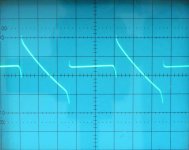
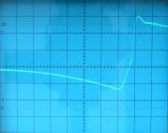
The repetitive signal frequency (step-shape signal) on any active divider output equals fDEM /4. In order to keep this frequency above the audio range, the DEM frequency should be at least 4 x 20KHz = 80 KHz.
First oscillogram shows the DEM oscillator signal, second oscillogram shows one of the transients in detail.
The DEM oscillator crosstalks with BCK and WS (that's why the free running DEM oscillator can lock to multiples of fs). This means that the jitter spectrum will be changed by it and this in turn may be audible. In other words, when the DEM frequency is changed and the active divider outputs are perfectly filtered, one could still hear its effect on sound quality through jitter contribution.
Referring to post #2738 Building the ultimate NOS DAC using TDA1541A, I would like to know if a lock condition is possible in NOS on 4 x fWS (176.4 kHz). I calculated the internal timing R for the above C values, and it seems that R is around 12.2 kohm. So the C giving 176.4 kHz fDEM might be around 465 pF. Will test it in the coming days…
Increasing the DEM timing cap value will work.
I am using a different DEM circuit in the SD8-player, here I can get low jitter at any DEM frequency I like. Circuit is as follows:
6K8 between pin 15 (-15V) and 16
6K8 between pin 15 (-15V) and 17
Timing cap between pin 16 and 17 (1n5 or lower).
The repetitive signal frequency (step-shape signal) on any active divider output equals fDEM /4. In order to keep this frequency above the audio range, the DEM frequency should be at least 4 x 20KHz = 80 KHz.
First oscillogram shows the DEM oscillator signal, second oscillogram shows one of the transients in detail.
The DEM oscillator crosstalks with BCK and WS (that's why the free running DEM oscillator can lock to multiples of fs). This means that the jitter spectrum will be changed by it and this in turn may be audible. In other words, when the DEM frequency is changed and the active divider outputs are perfectly filtered, one could still hear its effect on sound quality through jitter contribution.
Attachments
I was just about to try the DEM freq at around 80kHz on my old Rotel CD player and measured the capacitance on the present 700+kHz DEM setup and it's 128pF (101pF of FKP + variable 'air cap') - surprising thing is that the "lock" hasn't changed since I got it centred some time ago thru hot/cold/dry/humid days (no idea why it doesn't drift...)
This is the CD player with the Siemens 2uFs on the decoupling pins and the 4uF Solen on the MSBs (pins 13/18) - nothing neat or short tracks about this old much modified player , but still manages to sound rather good!
Will try the lower 80kHz freq with your 6k8 resistors and see how it sounds here too (will also try for the 88k1 multiple with a calculated 1024pF for a 'lock' here too)
Many thanks for your continuing development work, John, and for 'putting it up here' for all of us to try.
- Home
- Source & Line
- Digital Line Level
- Building the ultimate NOS DAC using TDA1541A