Hi studiostevus,
Yes.
Clock sources with fast transients need to be adapted for the slower TDA1541A (6.4 MHz limiting frequency) digital inputs. Failing to do so will cause surge currents during signal transients, dumping interference on the chip substrate.
This interference increases on-chip ground-bounce. This in turn increases trigger uncertainty and trigger uncertainly leads to increased on-chip jitter levels. The increased jitter levels are audible (jitter is audible).
The surge currents can also "back-fire" to driver / divider / clock circuits also leading to increased jitter levels in these clock sources.
In other words, the compatibility between clock source and TDA1541A will have direct effect on perceived sound quality as it changes jitter levels in both, clock source and TDA1541A.
In order to reduce ground-bounce caused by external (clock) signals we have to minimise clock frequency (NOS), minimise signal amplitude and make the clock signal compatible with the TDA1541A limiting frequency of 6.4 MHz.
In the latest TDA1541A prototype setup I use RC low pass filters / attenuators on all I2S signals. The C in these filters consists of TDA1541A input capacitance (12pF) plus PCB trace capacitance.
560R ... 1K.
- Did you notice any adverse consequences from such overshoot (like for example substrate bounce) ?
Yes.
Clock sources with fast transients need to be adapted for the slower TDA1541A (6.4 MHz limiting frequency) digital inputs. Failing to do so will cause surge currents during signal transients, dumping interference on the chip substrate.
This interference increases on-chip ground-bounce. This in turn increases trigger uncertainty and trigger uncertainly leads to increased on-chip jitter levels. The increased jitter levels are audible (jitter is audible).
The surge currents can also "back-fire" to driver / divider / clock circuits also leading to increased jitter levels in these clock sources.
In other words, the compatibility between clock source and TDA1541A will have direct effect on perceived sound quality as it changes jitter levels in both, clock source and TDA1541A.
In order to reduce ground-bounce caused by external (clock) signals we have to minimise clock frequency (NOS), minimise signal amplitude and make the clock signal compatible with the TDA1541A limiting frequency of 6.4 MHz.
In the latest TDA1541A prototype setup I use RC low pass filters / attenuators on all I2S signals. The C in these filters consists of TDA1541A input capacitance (12pF) plus PCB trace capacitance.
Are you using resistors or other means to counter overshoot?
560R ... 1K.
Hi studiostevus,
The rise time inside the TDA1541A is determined by its specified limiting frequency of 6.4 MHz. This corresponds with a signal rise time of approx. 56ns.
Each TDA1541A I2S input has a diode in series that stops conducting when the external signal amplitude exceeds approx. 1.4V. In other words, the external drive circuit is disconnected when the input diode stops conducting.
The positive transient is now determined by an internal CCS and input (stray) capacitance. In other words, the CCS needs some time to charge the input capacitance with the given CCS charge current.
This will be the fastest rise time that can be realised on the chip, regardless of the rise time of the external signal.
Connecting a low impedance to the BCK input doesn't help either (input series diode disconnects this impedance from the internal BCK circuit).
Here some examples of limiting frequency and rise time with different series resistor values with 12pF load:
2K2, 6.02 MHz, 60ns
1K8, 7.36 MHz, 49ns <
1K5, 8.84 MHz, 41ns
1K2, 11.052 MHz, 33ns
1K, 13.26 MHz, 27ns
820R, 16.17 MHz, 22ns
680R, 19.50 MHz, 18ns
560R, 23.68MHz, 15ns
470R, 28 MHz, 13ns
390R, 34 MHz, 10ns
330R, 40.19 MHz, 9ns
270R, 28.21 MHz, 7ns
220R, 60.28 MHz, 6ns
100R, 132 MHz, 2.7ns
47R, 282 MHz, 1.3ns
Based on this, the limiting series resistor value for TDA1541A BCK, WS, and DATA inputs would be 1K8
In order to create some margin (PCB trace capacitance) we can settle for approx. 1K. The exact value depends on the stray capacitance on the I2S signal lines and EMI (lower series resistor value increases immunity to EMI).
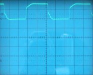
Another way to further reduce interference being dumped on the chip substrate is reducing I2S signal amplitude. I am now using BCK signal amplitude of 800mVpp with a DC offset of approx. 1V.
I attached an oscillogram of BCK.
560r....1k ?
That must be limiting rise time of the signal quite significantly. Especially on bck this could also cause trigger uncertainty i'd say, no?
The rise time inside the TDA1541A is determined by its specified limiting frequency of 6.4 MHz. This corresponds with a signal rise time of approx. 56ns.
Each TDA1541A I2S input has a diode in series that stops conducting when the external signal amplitude exceeds approx. 1.4V. In other words, the external drive circuit is disconnected when the input diode stops conducting.
The positive transient is now determined by an internal CCS and input (stray) capacitance. In other words, the CCS needs some time to charge the input capacitance with the given CCS charge current.
This will be the fastest rise time that can be realised on the chip, regardless of the rise time of the external signal.
Connecting a low impedance to the BCK input doesn't help either (input series diode disconnects this impedance from the internal BCK circuit).
Here some examples of limiting frequency and rise time with different series resistor values with 12pF load:
2K2, 6.02 MHz, 60ns
1K8, 7.36 MHz, 49ns <
1K5, 8.84 MHz, 41ns
1K2, 11.052 MHz, 33ns
1K, 13.26 MHz, 27ns
820R, 16.17 MHz, 22ns
680R, 19.50 MHz, 18ns
560R, 23.68MHz, 15ns
470R, 28 MHz, 13ns
390R, 34 MHz, 10ns
330R, 40.19 MHz, 9ns
270R, 28.21 MHz, 7ns
220R, 60.28 MHz, 6ns
100R, 132 MHz, 2.7ns
47R, 282 MHz, 1.3ns
Based on this, the limiting series resistor value for TDA1541A BCK, WS, and DATA inputs would be 1K8
In order to create some margin (PCB trace capacitance) we can settle for approx. 1K. The exact value depends on the stray capacitance on the I2S signal lines and EMI (lower series resistor value increases immunity to EMI).
Another way to further reduce interference being dumped on the chip substrate is reducing I2S signal amplitude. I am now using BCK signal amplitude of 800mVpp with a DC offset of approx. 1V.
I attached an oscillogram of BCK.
Attachments
Hi John (ecdesigns),
Regarding your post #4489 about hi-output I/V converter. I'd like to try it, in order to drive a PP EL84.
1. Can I replace BF862 with 2SK117GR? BF862 is not available here.
2. I'll apply to TDA1543. Supply and component value is as follow.
Supply Voltage: 250V
R source = 1.5k and connect to ground.
R drain = 44k
R I/V = 15k
No-signal current of TDA1543 aprox 1.3mA, adjust voltage on 1543's output = 3V, so bias current pass R source = 2mA
Current pass R drain = 5mA, so voltage over R I/V = 1.7mAx15k = 25.5V
Effective R I/V = 44x15/(44+15) = 11.186k
Vpp out = 29.08Vpp
I'll use this output from balance TDA1543, to drive a PP EL84. Your comment and suggestion is very appreciate.
Regards,
Art.
Hi Art,
BF862 max. VDS equals 20V so you would have to use a different JFET or MOSFET with suitable VDS.
For JFETS: use adjustable negative gate voltage.
For MOSFETs: use adjustable positive gate voltage.
Suitable MOSFET would be 2SK216 (200V VDS).
TDA1541A output voltage needs to be 0V, so we can use 0V as reference for the passive I/V resistor without the risk of clipping.
TDA1543 output voltage needs to be half the supply voltage so I/V resistor must be referenced to a 2V5 reference voltage. Then one might as well connect the I/V resistor to +V (say +70V) and use a coupling cap between I/V resistor and phase splitter.
Suggestion for approx. 27Vpp output signal:
70V +V supply (can be derived from tube HV using low noise voltage regulator).
12K passive I/V resistor between +70V and MOSFET drain.
8K2 between -15V and TDA1543 output (2mA extra bias current for MOSFET current buffer).
Coupling cap between MOSFET drain and phase splitter.
Push-Pull stage requires a phase splitter. One can also experiment with 2 x TDA1543 to generate balanced output signals, this way the phase splitter could be removed.
1. Can I replace BF862 with 2SK117GR? BF862 is not available here.
BF862 max. VDS equals 20V so you would have to use a different JFET or MOSFET with suitable VDS.
For JFETS: use adjustable negative gate voltage.
For MOSFETs: use adjustable positive gate voltage.
Suitable MOSFET would be 2SK216 (200V VDS).
2. I'll apply to TDA1543. Supply and component value is as follow.
TDA1541A output voltage needs to be 0V, so we can use 0V as reference for the passive I/V resistor without the risk of clipping.
TDA1543 output voltage needs to be half the supply voltage so I/V resistor must be referenced to a 2V5 reference voltage. Then one might as well connect the I/V resistor to +V (say +70V) and use a coupling cap between I/V resistor and phase splitter.
Suggestion for approx. 27Vpp output signal:
70V +V supply (can be derived from tube HV using low noise voltage regulator).
12K passive I/V resistor between +70V and MOSFET drain.
8K2 between -15V and TDA1543 output (2mA extra bias current for MOSFET current buffer).
Coupling cap between MOSFET drain and phase splitter.
Push-Pull stage requires a phase splitter. One can also experiment with 2 x TDA1543 to generate balanced output signals, this way the phase splitter could be removed.
Hi Output I/V for PP Tube
Hello John,
Thanks for your suggestion. I mean I'll use 2SK117GR.
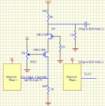
Yes. I have a balance TDA1543 Non-OS DAC. One TDA1543 for positive R/L signal and another for negative R/L signal. Now, it use op-amp I/V and get balance output to Push-Pull EL84 amplifier. I saw your hi-output I/V idea in post #4489.
I think I can remove op-amp I/V and driver tube for EL84 Amp. Then use your I/V and connect to EL84 directly.
The schematic is attached. Will this idea work? How do you think.
Best Regards,
Art.
Hello John,
Thanks for your suggestion. I mean I'll use 2SK117GR.
Yes. I have a balance TDA1543 Non-OS DAC. One TDA1543 for positive R/L signal and another for negative R/L signal. Now, it use op-amp I/V and get balance output to Push-Pull EL84 amplifier. I saw your hi-output I/V idea in post #4489.
I think I can remove op-amp I/V and driver tube for EL84 Amp. Then use your I/V and connect to EL84 directly.
The schematic is attached. Will this idea work? How do you think.
Best Regards,
Art.
Attachments
Hello John,
Thanks for your suggestion. I mean I'll use 2SK117GR.
Yes. I have a balance TDA1543 Non-OS DAC. One TDA1543 for positive R/L signal and another for negative R/L signal. Now, it use op-amp I/V and get balance output to Push-Pull EL84 amplifier. I saw your hi-output I/V idea in post #4489.
I think I can remove op-amp I/V and driver tube for EL84 Amp. Then use your I/V and connect to EL84 directly.
The schematic is attached. Will this idea work? How do you think.
Best Regards,
Art.
Art, the circuit you've designed will have an output impedance of about 11k ohms. That is quite high, and may result in noticeable high frequency roll-off, depending on the amount of lumped shunt capacitance of the interconnect together with that of the input of the next amplification stage.
Hi Art,
2SK117 (not connected to trimmer) gate must be connected to +5V in this setup, or you can leave it out for testing.
2SK117 VDS = 50V, so check if voltage doesn't exceed this limit.
Output impedance would be approx. 11.18K and could be too high as Ken Newton mentioned.
Output impedance can be reduced by increasing full-scale current (paralleling DAC chips) and lowering I/V resistor value.
You can also try placing a suitable unity gain buffer with low input capacitance and high input impedance between I/V resistor and EL84.
It would be better to create 2mA bias current by using say -15V supply and 9K series resistor. This way the impedance of the passive bias current source can be increased.
Hi Ken, John
Thank you very much for your suggestion.
Ken, output (after coupling cap) will be connected to EL84 by a 3-4 cm wire and EL84 have input capacitance just 10-12pF. Do you think the HF will be roll-off?
John, what's the benefit if the impedance of the passive bias current source increase? and Please suggest how to build -unity gain buffer with low input capacitance and high input impedance-. I' just know that tube and JFET have low input C and high input impedance, compare to Tr and MOSFET, but no idea how to.
Best Regards,
Art.
Ken, output (after coupling cap) will be connected to EL84 by a 3-4 cm wire and EL84 have input capacitance just 10-12pF. Do you think the HF will be roll-off?
Best Regards,
Art.
With such low shunt capacitance, the the -3dB frequency of this coupling will be in the vicinity of 800kHz, so you will not have any problem with audible HF roll-off.

Hi Dr H,
I use the charge-transfer supplies (regular or floating) in all my equipment for years now, even on power amps (with active devices suitable for the task) with very good performance. I have recommended them everywhere but it seems with little success...
In fact, it is hard to listen to non charge-transferred units once one gets used to the clean sound they provide...
Good luck,
M.
Hi Dr H,
I use the charge-transfer supplies (regular or floating) in all my equipment for years now, even on power amps (with active devices suitable for the task) with very good performance. I have recommended them everywhere but it seems with little success...
In fact, it is hard to listen to non charge-transferred units once one gets used to the clean sound they provide...
Good luck,
M.
Hi, Max,
Would you publish the schematic and parts list of the power amp scale implementation of the floating charge-transfer circuit? I often have A.C. line noise at my home, in the form of very audible 'buzzing' sound, so severe that I have been seriously considering powering even my power amp from a high capacity battery supply. Not to hijack John's thread, but I'd also be interested in reading any experience you might have with the subjective quality of charge-transfer power versus battery power. Please feel free to e-mail this information, if you would prefer to.
Hello John,
for the improvement of the TDA1541A-MKxx DAC you changed the power supply concept several times.
I'm a little confused concerning the use of the capacitance multiplier.
What is the advantage of a 4th order capacitance multiplier compared to a capacitance multiplier in plus lead and minus lead.
Does the 4th order capacitance multiplier consist of a chain of 4 RC elements (1st order) connected to the base of one darlington transistor located in the plus lead only?
If not could you please explain the structure.
Hi Dr. H and Ken,
Wow guys, you maybe ask too much from limited skills, but I will try to help. I mean, I can help the circuit to work but I cannot advice the optimal solution for each case. Anyway, I am sure -EC-, which is altruism personified, will jump in any minute.
For CD player just make the same circuit -EC- designed. Almost any mosfet will do, I imagine.
For a high power class A amp the demands of voltage and current will be huge for the mosfet and diodes, and will need to be heatsinked. Perhaps better try with normal diodes and not shottky, at first, because they can take more stress and are cheaper. I will tell you how I did the search: first investigate what are the demands for V and I of the amp; then entered my dealer's site (RS-components) and searched for the mosfet and shottkies that best suited the task (and were not hyperexpensive). You will need to buy high wattage resistances also, but I as said I am unable to tell what values are optimal, like gate input capacitance...etc.
I have never built a high power "floating charge transfer supply" but I am considering as a next project (after DX Blame and SSA) for a Makura's Power Follower "following" a high output DI M1 dac with variable I/V resistance: only one polarity needed. I only need the transformer. If I don't get it, I will make a regular charge transfer suply.
Buzz is a nightmare. I have been fighting with it on my main system (98 and 105db/W efficient transducers) for years and now I have acceptable low levels. I decided to rewire all the components for proper grounding, which would be my first advice. Only the amps are still pending...I think reading all the stuff about proper grounding (I did it but still have buzz, he, he) should be a requisite to become a member of the Forum that would save a lot of anger and frustration...once we are frustrated we cannot think correctly and chances are that we never solve the problem 
A tip that has helped me, if the buzz increases with increasing volume, the problem is "before" the preamp; if it is not modified, the problem is "after" the preamp. If it appears that the noise increases or decreases, depending on the source selected, the problem maybe the preamp itself...
That said, floating charge-transfer supply (for now on FCTS) is dangerous and will need proper double insulation technique.
For a double polarity FCTS you will need doubling -EC's- circuit. He published the circuit years ago. I will try to find it but I remember an 8 lead TX ( or two "center tappered" TXs in parallel) was needed. Again, you will need to look for suitable (V and I) Darlingtons and schottkies. A tip: FCTS doubles output V! so high voltage caps are needed and TX output V must be chosen accordingly.
Example: if you build one FCTS with a 9*2VAC TX (9-0/9-0) each rail will contribute with 9*1.44 minus diode loses so you will end with more or less a 22-0VDC FCTS...am I right EC?
Sorry guys, I am at work now and very busy. Will look for further info tomorrow.
Cheers,
M.
Wow guys, you maybe ask too much from limited skills, but I will try to help. I mean, I can help the circuit to work but I cannot advice the optimal solution for each case. Anyway, I am sure -EC-, which is altruism personified, will jump in any minute.
For CD player just make the same circuit -EC- designed. Almost any mosfet will do, I imagine.
For a high power class A amp the demands of voltage and current will be huge for the mosfet and diodes, and will need to be heatsinked. Perhaps better try with normal diodes and not shottky, at first, because they can take more stress and are cheaper. I will tell you how I did the search: first investigate what are the demands for V and I of the amp; then entered my dealer's site (RS-components) and searched for the mosfet and shottkies that best suited the task (and were not hyperexpensive). You will need to buy high wattage resistances also, but I as said I am unable to tell what values are optimal, like gate input capacitance...etc.
I have never built a high power "floating charge transfer supply" but I am considering as a next project (after DX Blame and SSA
) for a Makura's Power Follower "following" a high output DI M1 dac with variable I/V resistance: only one polarity needed. I only need the transformer. If I don't get it, I will make a regular charge transfer suply.Buzz is a nightmare. I have been fighting with it on my main system (98 and 105db/W efficient transducers) for years and now I have acceptable low levels. I decided to rewire all the components for proper grounding, which would be my first advice. Only the amps are still pending...I think reading all the stuff about proper grounding (I did it but still have buzz, he, he) should be a requisite to become a member of the Forum
that would save a lot of anger and frustration...once we are frustrated we cannot think correctly and chances are that we never solve the problem A tip that has helped me, if the buzz increases with increasing volume, the problem is "before" the preamp; if it is not modified, the problem is "after" the preamp. If it appears that the noise increases or decreases, depending on the source selected, the problem maybe the preamp itself...
That said, floating charge-transfer supply (for now on FCTS) is dangerous and will need proper double insulation technique.
For a double polarity FCTS you will need doubling -EC's- circuit. He published the circuit years ago. I will try to find it but I remember an 8 lead TX ( or two "center tappered" TXs in parallel) was needed. Again, you will need to look for suitable (V and I) Darlingtons and schottkies. A tip: FCTS doubles output V! so high voltage caps are needed and TX output V must be chosen accordingly.
Example: if you build one FCTS with a 9*2VAC TX (9-0/9-0) each rail will contribute with 9*1.44 minus diode loses so you will end with more or less a 22-0VDC FCTS...am I right EC?
Sorry guys, I am at work now and very busy. Will look for further info tomorrow.
Cheers,
M.
Last edited:
Buzz is a nightmare. I have been fighting with it on my main system (98 and 105db/W efficient transducers) for years and now I have acceptable low levels. I decided to rewire all the components for proper grounding, which would be my first advice....A tip that has helped me, if the buzz increases with increasing volume, the problem is "before" the preamp; if it is not modified, the problem is "after" the preamp. If it appears that the noise increases or decreases, depending on the source selected, the problem maybe the preamp itself...
Cheers,
M.
The buzzing I'm getting is not due to any ground loop problem, as I can disconnect the preamp and the buzz remains unaffected. Also, it's much worse at night than during the daytime. I can see the noise via my Tek digital scope, it is an approx. 2.5kHz sawtooth waveform riding the 60Hz line in periodic bursts. Ugly on the scope, ugly to hear.
Sorry to be silent. I got the flu.
Look at this high power shottky:
Schottky Rectifier Common Cathode Diode 90V 20A | eBay
Datasheet says 370pF capacitance.
The other day I re-read the thread and could not find the double polarity FCTS. I will try to figure out a schematic.
Good luck.
M.
Look at this high power shottky:
Schottky Rectifier Common Cathode Diode 90V 20A | eBay
Datasheet says 370pF capacitance.
The other day I re-read the thread and could not find the double polarity FCTS. I will try to figure out a schematic.
Good luck.
M.

- Home
- Source & Line
- Digital Line Level
- Building the ultimate NOS DAC using TDA1541A