Hi s3tup,
The description DEM reclocking is indeed incorrect, DEM oscillator synchronization would be a better description.
The DEM (Dynamic Element Matching) circuit dynamically matches the passive divider output currents for the 6 MSBs only. Philips developed this technique in order to offer high accuracy without the need for expensive (LASER) trimming.
The remaining 10 LSBs are -not- corrected by DEM and are derived from passive dividers. Passive dividers are used to derive binary weighted bit currents (2mA, 1mA, 0.5mA, 0.25mA and so on) from a single current reference source. These binary weighted bit currents are later combined by bit switches to obtain 65,536 possible current levels between 0 and -4mA. With no signal applied, the DAC bias current equals -2mA.
The DEM clock drives shift registers that in turn control an active divider switch matrix. The outputs of these active dividers are averaged / filtered by a RC filter. The active divider outputs provide a constant filtered DC current so there is basically no direct need to complete a full switch matrix cycle for each sample duration.
All an active divider does is averaging between 4 unmatched input currents from a passive divider, providing 4 closely matched output currents at the switch matrix outputs.
So it basically does this:
I out 1 = (I in1 / 4) + (I in 2 /4) + (I in3 / 4) + (I in4 /4)
I out 2 = (I in2 / 4) + (I in 3 /4) + (I in4 / 4) + (I in1 /4)
I out 3 = (I in3 / 4) + (I in 4 /4) + (I in1 / 4) + (I in2 /4)
I out 4 = (I in4 / 4) + (I in 1 /4) + (I in2 / 4) + (I in3 /4)
Addition is done by changing switch positions in the switch matrix, division is done by so called time division (each switch is closed for a specified amount of time).
This also means that slightest deviations in DEM clock rate (jitter) will lead to slight time division errors and thus reduced matching. This is corrected to certain extent by the RC filter.
Unfortunately a 1st order RC filter like used on the active divider outputs offers insufficient attenuation of ripple current (must remain well below 40nA in order not to mask LSB).
Since the filter only offers 6dB attenuation, ripple current always seeps through and leads to an unwanted ripple current on the MSBs. So DEM circuit accuracy depends heavily on how effectively this ripple current can be attenuated. Note that 1 LSB represents only 40nA.
Other problem is that all capacitors distort (they are imperfect). Some major causes are mechanical resonances in charged foils, piezoelectric effects, and low level signal processing limitations.
Ripple current is proportional to passive divider mismatch, so more accurate DAC chips like the TDA1541A-S2 or DAC chips from more recent production series should provide lower ripple current under similar conditions.
Ground noise is also directly coupled into the active divider outputs through the filter cap (low impedance). So in practice it will be extremely difficult to get ripple current levels at the active divider output down to acceptable levels. This is why TDA1541A applications are extremely critical and many conventional TDA1541A applications will certainly suffer from reduced low level performance. This is not caused by the DAC chip but is simply a result of poor design.
Higher value filter caps could be a possible solution provided their reactance is low enough and traces are kept short enough to maintain required low impedance at RF (200 KHz and up). Most physically large decoupling caps with long traces fail to offer low enough impedance for effective decoupling at RF.
Apart from the active divider output ripple, there will also be inter-modulation / crosstalk between DEM oscillator and the DAC output signal and DEM oscillator and I2S timing signals.
Listening tests clearly showed that higher DEM clock rates lead to cleaner more refined sound reproduction.
TDA1541A limit frequency (for all circuits) is around 7 MHz this includes the DEM oscillator.
Since I wanted to avoid inter-modulation between BCK and DEM oscillator I changed the value of the DEM oscillator timing cap to approx. 33pF and then synchronized the DEM oscillator with 2.8224 MHz BCK signal.
Forcing the DEM oscillator (triggering) failed as it caused spurious oscillations and interference being dumped on the chip substrate.
DEM oscillator synchronization is extremely critical and since there is no provision for an external DEM clock signal we have to use the timing cap inputs one way or the other.
Simply connecting BCK to pins 16 or 17 using a coupling capacitor will not work for sure, it will disrupt DEM oscillator circuit operation and degrade BCK signal (increased BCK jitter). Distortion would be accordingly.
what they mean by "DEM reclocking" is not the reclocking itself, but forcing TDA's "dynamic element matching" circuitry to run with external clock. So the DEM averaging will always contain at least 4 steps for each sample (herein it's rate should be 4Fs or greater, there are just 4 positions of current dividers).
The description DEM reclocking is indeed incorrect, DEM oscillator synchronization would be a better description.
The DEM (Dynamic Element Matching) circuit dynamically matches the passive divider output currents for the 6 MSBs only. Philips developed this technique in order to offer high accuracy without the need for expensive (LASER) trimming.
The remaining 10 LSBs are -not- corrected by DEM and are derived from passive dividers. Passive dividers are used to derive binary weighted bit currents (2mA, 1mA, 0.5mA, 0.25mA and so on) from a single current reference source. These binary weighted bit currents are later combined by bit switches to obtain 65,536 possible current levels between 0 and -4mA. With no signal applied, the DAC bias current equals -2mA.
The DEM clock drives shift registers that in turn control an active divider switch matrix. The outputs of these active dividers are averaged / filtered by a RC filter. The active divider outputs provide a constant filtered DC current so there is basically no direct need to complete a full switch matrix cycle for each sample duration.
All an active divider does is averaging between 4 unmatched input currents from a passive divider, providing 4 closely matched output currents at the switch matrix outputs.
So it basically does this:
I out 1 = (I in1 / 4) + (I in 2 /4) + (I in3 / 4) + (I in4 /4)
I out 2 = (I in2 / 4) + (I in 3 /4) + (I in4 / 4) + (I in1 /4)
I out 3 = (I in3 / 4) + (I in 4 /4) + (I in1 / 4) + (I in2 /4)
I out 4 = (I in4 / 4) + (I in 1 /4) + (I in2 / 4) + (I in3 /4)
Addition is done by changing switch positions in the switch matrix, division is done by so called time division (each switch is closed for a specified amount of time).
This also means that slightest deviations in DEM clock rate (jitter) will lead to slight time division errors and thus reduced matching. This is corrected to certain extent by the RC filter.
Unfortunately a 1st order RC filter like used on the active divider outputs offers insufficient attenuation of ripple current (must remain well below 40nA in order not to mask LSB).
Since the filter only offers 6dB attenuation, ripple current always seeps through and leads to an unwanted ripple current on the MSBs. So DEM circuit accuracy depends heavily on how effectively this ripple current can be attenuated. Note that 1 LSB represents only 40nA.
Other problem is that all capacitors distort (they are imperfect). Some major causes are mechanical resonances in charged foils, piezoelectric effects, and low level signal processing limitations.
Ripple current is proportional to passive divider mismatch, so more accurate DAC chips like the TDA1541A-S2 or DAC chips from more recent production series should provide lower ripple current under similar conditions.
Ground noise is also directly coupled into the active divider outputs through the filter cap (low impedance). So in practice it will be extremely difficult to get ripple current levels at the active divider output down to acceptable levels. This is why TDA1541A applications are extremely critical and many conventional TDA1541A applications will certainly suffer from reduced low level performance. This is not caused by the DAC chip but is simply a result of poor design.
Higher value filter caps could be a possible solution provided their reactance is low enough and traces are kept short enough to maintain required low impedance at RF (200 KHz and up). Most physically large decoupling caps with long traces fail to offer low enough impedance for effective decoupling at RF.
The DEM isn't supposed to run this way, and it's native frequency is around 300-700kHz, self oscillating and running free.
Apart from the active divider output ripple, there will also be inter-modulation / crosstalk between DEM oscillator and the DAC output signal and DEM oscillator and I2S timing signals.
Listening tests clearly showed that higher DEM clock rates lead to cleaner more refined sound reproduction.
TDA1541A limit frequency (for all circuits) is around 7 MHz this includes the DEM oscillator.
Since I wanted to avoid inter-modulation between BCK and DEM oscillator I changed the value of the DEM oscillator timing cap to approx. 33pF and then synchronized the DEM oscillator with 2.8224 MHz BCK signal.
Forcing the DEM oscillator (triggering) failed as it caused spurious oscillations and interference being dumped on the chip substrate.
DEM oscillator synchronization is extremely critical and since there is no provision for an external DEM clock signal we have to use the timing cap inputs one way or the other.
What studiostevus did is connected the BCLK directly to DEM, and forced it to run on 2.8MHz which is a bit more than 300-700kHz, hence his strong suspectism.
Simply connecting BCK to pins 16 or 17 using a coupling capacitor will not work for sure, it will disrupt DEM oscillator circuit operation and degrade BCK signal (increased BCK jitter). Distortion would be accordingly.
nowhere,
what they mean by "DEM reclocking" is not the reclocking itself, but forcing TDA's "dynamic element matching" circuitry to run with external clock. So the DEM averaging will always contain at least 4 steps for each sample (herein it's rate should be 4Fs or greater, there are just 4 positions of current dividers).
The DEM isn't supposed to run this way, and it's native frequency is around 300-700kHz, self oscillating and running free.
What studiostevus did is connected the BCLK directly to DEM, and forced it to run on 2.8MHz which is a bit more than 300-700kHz, hence his strong suspectism.
Does your explanation disprove my statement that clock problems affect more or less the same both weak and strong signals ?
Simply connecting BCK to pins 16 or 17 using a coupling capacitor will not work for sure, it will disrupt DEM oscillator circuit operation and degrade BCK signal (increased BCK jitter). Distortion would be accordingly.
I realize that..
") . my setup is as follows:
. my setup is as follows:BCK to pin 16 via a 12k resistor in series, with a 2k2 resistor to -15V in parallel.
pin16 and pin17 connected to each other using 33pf cap.
nowhere, you are right, jitter affects all signal levels.
I've tried to clear-out that the "reclocking" word in "DEM reclocking" statement is more about syncing the DEM to Fs*X rate rather than fighting the jitter.
-ecdesigns-,
It's kinda weird you've got better results with higher DEM rate...
By increasing the DEM rate 4 times, you increase the amount of emissions by the same 4 times (slew rates stay the same, rate of changes increase 4x, so amount increases 4x).
4x higher frequency = 4x better coupling into surrounding circuits (stray capacitance stays the same, higher frequency = better coupling).
By increasing DEM rate, you go higher into RF zone with more uncontrollable parasitics around.
Maybe it's due to undersized DEM-decoupling capacitors...
When you rise the DEM frequency 4x times, you go to lower impedance zone for DEM caps = 1/4 of original impedance, hence the better decoupling.
r(impedance)=1/2*Pi*f*c for low-frequency part of "V"-shaped capacitor impedance graph.
DEM synchronisation to fs has very big problem, error after DEM work has no averaging! (as it has when DEM clock is asynchronous to fs).
And if you "cook" you 1541 maximally good, the resulting sound quality with DEM sync is definitely worse then with asynchronous (free running) DEM clock.
And if you "cook" you 1541 maximally good, the resulting sound quality with DEM sync is definitely worse then with asynchronous (free running) DEM clock.
Nazar_lv, even if we cycle thru all 4 positions during the LRCLK?
It should perfectly average for single sample...
But it won't average for a couple of samples. The error in DEM will be sample-correlated and will be constant for every same sample.
DEM should run freely if we want to get averaging between samples too...
It should perfectly average for single sample...
But it won't average for a couple of samples. The error in DEM will be sample-correlated and will be constant for every same sample.
DEM should run freely if we want to get averaging between samples too...
Not strictly related to DEM, I want to point to the important role of MSB. It is also called "sign bit", and it keeps changing on/off when the analog signal is at the lowest level. In contrast, the next significant bit changes at +/- 1/2 full scale, so it has no influence on low level analog signals. My conclusion is that the circuit associated to MSB should be treated with much higher percision that the other passive dividers.
Hi Nazar_Iv,
There is no need to complete a DEM cycle "within" a sample period. CD players with this chip and 4 * fs run on 176.4 Khz sample rate.
DEM clock equals approx. 200 KHz and a complete DEM cycle takes 4 clock pulses to complete (approx. 50 KHz rate)
So it typically takes approx. 3.5 samples to complete a DEM clock cycle.
It is possible to use 2KHz DEM clock rate with 10uF decoupling caps or 200 Hz DEM clock rate with 100uF decoupling caps or 44.1 KHz DEM clock rate with 470nF decoupling caps.
The trick is the decoupling cap that smoothens the output signal similar to a smoothing cap placed after a rectifier.
This results in an average bit current (DC) with very small ripple current (AC) super imposed on it.
However, these small ripple currents end up on the DAC outputs and mess-up the output signal (inter-modulation).
TDA1541A is based on current mode logic (CML). Property of current mode logic is that power consumption remains fairly constant (but higher compared to CMOS) regardless of clock frequency. So nothing gets "cooked". I also stay well within TDA1541A limit frequency of approx. 7 MHz so reliable switching is guaranteed.
it is not so easy to correctly synchronize the DEM oscillator with an external clock. So it is likely that a synchronized DEM clock circuit simply doesn't work as it should. Then "synchronized" DEM clock circuits often perform worse compared to the Philips data sheet application.
This however doesn't mean that all DEM clock synchronization circuits perform bad by definition.
DEM synchronisation to fs has very big problem, error after DEM work has no averaging!
There is no need to complete a DEM cycle "within" a sample period. CD players with this chip and 4 * fs run on 176.4 Khz sample rate.
DEM clock equals approx. 200 KHz and a complete DEM cycle takes 4 clock pulses to complete (approx. 50 KHz rate)
So it typically takes approx. 3.5 samples to complete a DEM clock cycle.
It is possible to use 2KHz DEM clock rate with 10uF decoupling caps or 200 Hz DEM clock rate with 100uF decoupling caps or 44.1 KHz DEM clock rate with 470nF decoupling caps.
The trick is the decoupling cap that smoothens the output signal similar to a smoothing cap placed after a rectifier.
This results in an average bit current (DC) with very small ripple current (AC) super imposed on it.
However, these small ripple currents end up on the DAC outputs and mess-up the output signal (inter-modulation).
And if you "cook" you 1541 maximally good, the resulting sound quality with DEM sync is definitely worse then with asynchronous (free running) DEM clock.
TDA1541A is based on current mode logic (CML). Property of current mode logic is that power consumption remains fairly constant (but higher compared to CMOS) regardless of clock frequency. So nothing gets "cooked". I also stay well within TDA1541A limit frequency of approx. 7 MHz so reliable switching is guaranteed.
it is not so easy to correctly synchronize the DEM oscillator with an external clock. So it is likely that a synchronized DEM clock circuit simply doesn't work as it should. Then "synchronized" DEM clock circuits often perform worse compared to the Philips data sheet application.
This however doesn't mean that all DEM clock synchronization circuits perform bad by definition.
not intermodulation, multiplication!mess-up the output signal (inter-modulation).
regards,
Nazar
Hi oshifis,
The active divider bit outputs have RC filters installed. With approx. 500R on-chip resistor and 100nF filter cap we get a corner frequency of around 3000 Hz. The DEM clock rate equals 200,000 Hz. The ripple current frequency at the active divider outputs equals 200 KHz for the single outputs and 100 KHz for the paralleled outputs. Both are well above the filter corner frequency so we should end up with a clean filtered DC current with very low ripple at the output if the DEM clock was the only clock signal present on the chip.
But there are other (lower frequency) signals present on the DAC chip that can crosstalk to the bit outputs. So one could still end up with low frequency ripple current on the active divider outputs that falls within the audio band.
This unwanted effect can be reduced by increasing filter cap values, thus lowering filter corner frequency.
Note that the DC bit current outputs (active divider bit current outputs included) are selected by -additional- bit switches that combine currents from the 16 binary weighted DC bit currents in order to produce the actual DAC output current .
In practice, higher value filter caps offer subtle improvements by attenuating lower frequencies like WS crosstalk that might otherwise seep through. Above a certain value (around 10uF for 200 KHz DEM clock rate) little or no improvement is achieved. With 10uF filter cap we would get a corner frequency of around 30 Hz.
Also keep in mind that MSB is directly derived from the current reference source and therefore has no ripple. The next 5 MSBs are derived from 3 active dividers. The 10 LSBs are derived from a passive divider (no correction) but they are fed by the filtered output current of the last active divider. As this current is divided down, the residual ripple current on it is also divided. All derived bit currents "follow" the current reference source. TDA1541A is designed such way that glitch energy stays below 0.25 LSB at MSB change (1000000000000000 > 0111111111111111).
DEM corrects the -differences- between the 4 unmatched input currents. Typical matching tolerance equals approx. 0.1%. So an input current of 1mA can have a typical deviation of 1uA or 1000nA.
In order to get errors below 1 LSB (40nA) differences between switch intervals must stay below 4%. For 0.25 LSB error the frequency shouldn't fluctuate more than 1%. So for a 200 KHz DEM clock the allowed frequency fluctuations should stay below 2000 Hz or 500us peak to peak.
So it takes a pretty lousy DEM clock in order to exceed these values
The resulting DC bit current has -no- relation with fs, compare it with the DC output voltage of a switch-mode power supply, powering an oscillator running at a different frequency compared to the SMPS.
It is irrelevant if the DEM clock is synced with another clock or not. The operation (averaging between 4 input currents) remains effective as long as the time intervals between switch changes are equal (within certain tolerances).
In the MK11 and MK12 I use 1uF filter cap, with 500R this results in corner frequency of around 300 Hz
I use a free running DEM oscillator with timing cap. I reduced capacitor value so it oscillates around 3 MHz, it is then synchronized -not triggered- with the bit clock BCK (2.8224 MHz). So DEM clock jitter basically remains similar to a correctly functioning free running DEM oscillator. In order to meet 1% frequency stability, the DEM clock should not fluctuate more than 28 KHz or 35us peak to peak jitter. In practice it is no problem to achieve much lower values, this means I fully meet the conditions to stay well below 0.25 LSB error.
In short, when the DEM clock gets a reasonable clock signal and suitable filter caps are installed the bit errors introduced by the DEM circuit stay well below 0.25 LSB. It also doesn't matter if the DEM clock is synchronized or not.
So why did I synchronize the DEM clock with the bit clock?
This has to do with on-chip crosstalk and the effect on sample timing (jitter) among other things. Also note that I use NOS so I have 44.1 KHz word clock and 2.8224 Mhz bit clock instead of the 4 * OS variant where we have 176.4 KHz word clock and 5.6448 MHz bit clock.
I2S timing signals BCK and WS can be viewed as a fundamentals with harmonics. The DEM clock can also be viewed as a fundamental with harmonics. When these are added together (crosstalk) we get inter-modulation:
Intermodulation - Wikipedia, the free encyclopedia
So by using the same frequency as bit clock or word clock for the DEM clock, we can prevent inter-modulation and its unwanted side effects.
So with NOS I now have two options:
Using word clock (44.1 KHz DEM clock), or bit clock (2.8224 MHz DEM clock). Other multiples of fs are not desired as these wouldn't be equal to the already present clock signals WS and BCK.
With 44.1 KHz DEM clock rate I would have to increase decoupling cap values significantly.
So I picked the remaining bit clock (2.8224 MHz).
explain why asynchronous DEM clocking is better than synchronous, provided that fDEM >> fs ? Or John should explain the opposite... Also is the following equation correct? fDEM >= n x (4 x fs), where n = 1, 2,
The active divider bit outputs have RC filters installed. With approx. 500R on-chip resistor and 100nF filter cap we get a corner frequency of around 3000 Hz. The DEM clock rate equals 200,000 Hz. The ripple current frequency at the active divider outputs equals 200 KHz for the single outputs and 100 KHz for the paralleled outputs. Both are well above the filter corner frequency so we should end up with a clean filtered DC current with very low ripple at the output if the DEM clock was the only clock signal present on the chip.
But there are other (lower frequency) signals present on the DAC chip that can crosstalk to the bit outputs. So one could still end up with low frequency ripple current on the active divider outputs that falls within the audio band.
This unwanted effect can be reduced by increasing filter cap values, thus lowering filter corner frequency.
Note that the DC bit current outputs (active divider bit current outputs included) are selected by -additional- bit switches that combine currents from the 16 binary weighted DC bit currents in order to produce the actual DAC output current .
In practice, higher value filter caps offer subtle improvements by attenuating lower frequencies like WS crosstalk that might otherwise seep through. Above a certain value (around 10uF for 200 KHz DEM clock rate) little or no improvement is achieved. With 10uF filter cap we would get a corner frequency of around 30 Hz.
Also keep in mind that MSB is directly derived from the current reference source and therefore has no ripple. The next 5 MSBs are derived from 3 active dividers. The 10 LSBs are derived from a passive divider (no correction) but they are fed by the filtered output current of the last active divider. As this current is divided down, the residual ripple current on it is also divided. All derived bit currents "follow" the current reference source. TDA1541A is designed such way that glitch energy stays below 0.25 LSB at MSB change (1000000000000000 > 0111111111111111).
DEM corrects the -differences- between the 4 unmatched input currents. Typical matching tolerance equals approx. 0.1%. So an input current of 1mA can have a typical deviation of 1uA or 1000nA.
In order to get errors below 1 LSB (40nA) differences between switch intervals must stay below 4%. For 0.25 LSB error the frequency shouldn't fluctuate more than 1%. So for a 200 KHz DEM clock the allowed frequency fluctuations should stay below 2000 Hz or 500us peak to peak.
So it takes a pretty lousy DEM clock in order to exceed these values
The resulting DC bit current has -no- relation with fs, compare it with the DC output voltage of a switch-mode power supply, powering an oscillator running at a different frequency compared to the SMPS.
It is irrelevant if the DEM clock is synced with another clock or not. The operation (averaging between 4 input currents) remains effective as long as the time intervals between switch changes are equal (within certain tolerances).
In the MK11 and MK12 I use 1uF filter cap, with 500R this results in corner frequency of around 300 Hz
I use a free running DEM oscillator with timing cap. I reduced capacitor value so it oscillates around 3 MHz, it is then synchronized -not triggered- with the bit clock BCK (2.8224 MHz). So DEM clock jitter basically remains similar to a correctly functioning free running DEM oscillator. In order to meet 1% frequency stability, the DEM clock should not fluctuate more than 28 KHz or 35us peak to peak jitter. In practice it is no problem to achieve much lower values, this means I fully meet the conditions to stay well below 0.25 LSB error.
In short, when the DEM clock gets a reasonable clock signal and suitable filter caps are installed the bit errors introduced by the DEM circuit stay well below 0.25 LSB. It also doesn't matter if the DEM clock is synchronized or not.
So why did I synchronize the DEM clock with the bit clock?
This has to do with on-chip crosstalk and the effect on sample timing (jitter) among other things. Also note that I use NOS so I have 44.1 KHz word clock and 2.8224 Mhz bit clock instead of the 4 * OS variant where we have 176.4 KHz word clock and 5.6448 MHz bit clock.
I2S timing signals BCK and WS can be viewed as a fundamentals with harmonics. The DEM clock can also be viewed as a fundamental with harmonics. When these are added together (crosstalk) we get inter-modulation:
Intermodulation - Wikipedia, the free encyclopedia
So by using the same frequency as bit clock or word clock for the DEM clock, we can prevent inter-modulation and its unwanted side effects.
So with NOS I now have two options:
Using word clock (44.1 KHz DEM clock), or bit clock (2.8224 MHz DEM clock). Other multiples of fs are not desired as these wouldn't be equal to the already present clock signals WS and BCK.
With 44.1 KHz DEM clock rate I would have to increase decoupling cap values significantly.
So I picked the remaining bit clock (2.8224 MHz).
Last edited:
Hi John,
what are your latest findings to synchronize the DEM clock with the bit clock?
CAP between Pin 16 and Pin17: (C=33pF Ceramic NPO)
Serial resistor between Pin2 (BCK) and Pin16: R=?? (BCK 0V/1.8V)
Is a resistor between Pin16 (Pin17) and -15V still required, if yes which value?
what are your latest findings to synchronize the DEM clock with the bit clock?
CAP between Pin 16 and Pin17: (C=33pF Ceramic NPO)
Serial resistor between Pin2 (BCK) and Pin16: R=?? (BCK 0V/1.8V)
Is a resistor between Pin16 (Pin17) and -15V still required, if yes which value?
Well have a look here....
Upper trace: pin16 (dem)
Lower trace: pin bck
Doesnt look good.... Does it?
Upper trace: pin16 (dem)
Lower trace: pin bck
Doesnt look good.... Does it?
An externally hosted image should be here but it was not working when we last tested it.
Instead of tinkering with these tweaks, why not to reduce the main source of troubles/crosstalk - the speed?
With NOS you can reduce the bitclock down to 700kHz range 44100x16.
16 bits, simultaneous load, and with better jitter performance = dedicated low-jitterish WS input. You'll need to tinker with CPLD instead.
With NOS you can reduce the bitclock down to 700kHz range
44100x16.16 bits, simultaneous load, and with better jitter performance = dedicated low-jitterish WS input. You'll need to tinker with CPLD instead.
Hi JOSI1,
Like I mentioned in previous post, DEM clock can be synchronized with either BCK or WS.
In previous designs I triggered or synchronized the DEM clock with BCK.
This has some disadvantages as s3tup pointed out in post #4405.
Electronic switches in active divider cause switching spikes on the averaged output signal. These spikes have specific pulse width. The higher the DEM clock rate the more these switching spikes will dominate the active divider output signal shape.
It is also important to keep the sample steady current at the DAC output as clean as possible. The biggest problem here is the required BCK signal that puts noise (switching spikes) of 64 pulses on each sample. This results in a sample current with 128 "spikes" on top of it (on-chip crosstalk).
When synchronizing the DEM clock with BCK, there will always be a certain phase difference between these two frequencies. This is caused by DEM oscillator properties and propagation delays. This means that apart from the 128 spikes of BCK, we get another 128 spikes from the DEM clock so 256 spikes in total on BCK. Ideal situation would be a DAC with parallel inputs so we could get rid of the bit clock switching interference.
In case of the Philips data sheet application we get 128 spikes from BCK and approx. 9 spikes from the free running 200 KHz DEM clock that will constantly move position with respect to the BCK switching spikes.
Cleanest sample steady current could be obtained by synchronizing the DEM clock with WS, then we would add only 2 fixed switching spikes to the already present 128 spikes from BCK (130 switching spikes in total). This means that one DEM cycle (4 switch changes) is completed after every 4 samples.
Other advantage is that the filter caps and filter circuit become less critical as DEM clock rate is now reduced to 44.1 KHz (NOS).
Based on filter cap value of 100nF @ 200,000 Hz, DEM clock rate of 44,100 Hz would require 470nF filter caps (closest value). Since I already had 1uF filter caps installed I could easily test 44.1 KHz DEM clock with minimum changes to the existing circuit.
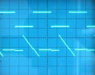
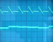
I attached an oscillogram showing WS (44.1 KHz) upper trace (measured at pin 1), and the synchronized DEM oscillator signal.
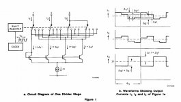
The second oscillogram shows the DEM oscillator signal (upper trace) and one active divider output with 1uF filter cap removed (second channel). Passive divider output current mismatch translates to a step current that's also described in TDA1540 data sheet and IEEE journal of semiconductors. I attached a copy of active divider stage and output current waveform.
One can see that the switching spikes are relatively short compared to the time between switch matrix changes. What we basically see here is a repeated sequence of unmatched input bit currents 1, 2, 3, and 4 that appear at the output of the 4-way electronic switch as it scans through all 4 positions at a rate of 44.1 KHz. Each of the 4 active divider outputs has such an electronic 4-way switch. This way each of the 4 outputs can average between each of the 4 inputs.
The higher the passive divider output current mismatch, the higher the step signal amplitude. Scope setting equals 2mV/div, probe 1:10. So the ripple current is actually rather small. The DEM oscillator causes crosstalk on the passive divider outputs (positive and negative spikes on the active divider outputs). These are just barely visible on the second oscillogram because the DEM clock frequency is very low compared to the given switching spike pulse width.
After re-connecting the filter capacitor, ripple voltage at the active divider output drops well below scope noise floor and we get a pure DC current.
The DEM circuit ensures that the 6 MSBs plus the input current for the 10 bit passive current divider always remain very closely matched, despite on-chip tolerances / chip aging. Keep in mind that even slightest errors in MSBs also lead to errors in the LSB range. So all bits contribute to the final bit accuracy.
The DEM oscillator now oscillates on the timing capacitor again, so 2K2 resistors need to be removed. For synchronization with WS, 33pF timing cap value is no longer valid.
what are your latest findings to synchronize the DEM clock with the bit clock?
Like I mentioned in previous post, DEM clock can be synchronized with either BCK or WS.
In previous designs I triggered or synchronized the DEM clock with BCK.
This has some disadvantages as s3tup pointed out in post #4405.
Electronic switches in active divider cause switching spikes on the averaged output signal. These spikes have specific pulse width. The higher the DEM clock rate the more these switching spikes will dominate the active divider output signal shape.
It is also important to keep the sample steady current at the DAC output as clean as possible. The biggest problem here is the required BCK signal that puts noise (switching spikes) of 64 pulses on each sample. This results in a sample current with 128 "spikes" on top of it (on-chip crosstalk).
When synchronizing the DEM clock with BCK, there will always be a certain phase difference between these two frequencies. This is caused by DEM oscillator properties and propagation delays. This means that apart from the 128 spikes of BCK, we get another 128 spikes from the DEM clock so 256 spikes in total on BCK. Ideal situation would be a DAC with parallel inputs so we could get rid of the bit clock switching interference.
In case of the Philips data sheet application we get 128 spikes from BCK and approx. 9 spikes from the free running 200 KHz DEM clock that will constantly move position with respect to the BCK switching spikes.
Cleanest sample steady current could be obtained by synchronizing the DEM clock with WS, then we would add only 2 fixed switching spikes to the already present 128 spikes from BCK (130 switching spikes in total). This means that one DEM cycle (4 switch changes) is completed after every 4 samples.
Other advantage is that the filter caps and filter circuit become less critical as DEM clock rate is now reduced to 44.1 KHz (NOS).
Based on filter cap value of 100nF @ 200,000 Hz, DEM clock rate of 44,100 Hz would require 470nF filter caps (closest value). Since I already had 1uF filter caps installed I could easily test 44.1 KHz DEM clock with minimum changes to the existing circuit.
I attached an oscillogram showing WS (44.1 KHz) upper trace (measured at pin 1), and the synchronized DEM oscillator signal.
The second oscillogram shows the DEM oscillator signal (upper trace) and one active divider output with 1uF filter cap removed (second channel). Passive divider output current mismatch translates to a step current that's also described in TDA1540 data sheet and IEEE journal of semiconductors. I attached a copy of active divider stage and output current waveform.
One can see that the switching spikes are relatively short compared to the time between switch matrix changes. What we basically see here is a repeated sequence of unmatched input bit currents 1, 2, 3, and 4 that appear at the output of the 4-way electronic switch as it scans through all 4 positions at a rate of 44.1 KHz. Each of the 4 active divider outputs has such an electronic 4-way switch. This way each of the 4 outputs can average between each of the 4 inputs.
The higher the passive divider output current mismatch, the higher the step signal amplitude. Scope setting equals 2mV/div, probe 1:10. So the ripple current is actually rather small. The DEM oscillator causes crosstalk on the passive divider outputs (positive and negative spikes on the active divider outputs). These are just barely visible on the second oscillogram because the DEM clock frequency is very low compared to the given switching spike pulse width.
After re-connecting the filter capacitor, ripple voltage at the active divider output drops well below scope noise floor and we get a pure DC current.
The DEM circuit ensures that the 6 MSBs plus the input current for the 10 bit passive current divider always remain very closely matched, despite on-chip tolerances / chip aging. Keep in mind that even slightest errors in MSBs also lead to errors in the LSB range. So all bits contribute to the final bit accuracy.
CAP between Pin 16 and Pin17: (C=33pF Ceramic NPO) Serial resistor between Pin2 (BCK) and Pin16: R=?? (BCK 0V/1.8V) Is a resistor between Pin16 (Pin17) and -15V still required, if yes which value?
The DEM oscillator now oscillates on the timing capacitor again, so 2K2 resistors need to be removed. For synchronization with WS, 33pF timing cap value is no longer valid.
Attachments
- Home
- Source & Line
- Digital Line Level
- Building the ultimate NOS DAC using TDA1541A