Hi studiostevus,
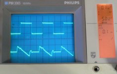
This change was the result of continuous attempts to improve the TDA1541A application. The DEM clock now runs on an external timing capacitor between pins 16 and 17. It is synchronized by the attenuated 2.8224 MHz BCK signal (soft-sync). First picture shows BCK (upper channel) and the signal on TDA1541A pin 17. It shows the DEM oscillator is synchronized with BCK while running on an external timing cap.
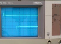
I use a digital audio source (SD8-transport) that was specifically designed (hardware & software) to provide low interference and jitter levels. I attached a second photograph to illustrate this, the photograph shows SD8-transport I2S data signal output.
TDA1541A samples WS and DATA signals with BCK, so synchronous reclocking with BCK already takes place on the chip.
Hi John,
If I see correctly, you are currently only using 1 DEM reclocking line (I guess synchronized and attenuated BCK). What triggered this change? Is the other pin now left floating?
This change was the result of continuous attempts to improve the TDA1541A application. The DEM clock now runs on an external timing capacitor between pins 16 and 17. It is synchronized by the attenuated 2.8224 MHz BCK signal (soft-sync). First picture shows BCK (upper channel) and the signal on TDA1541A pin 17. It shows the DEM oscillator is synchronized with BCK while running on an external timing cap.
Also WS and DATA seem to be straight from the source module, without additional reclocking via MCLK/BCK. Does this reduce jitter compared to reclocking based on MCLK/BCK? I guess you completely rely then on edge-triggering inside the TDA?
I use a digital audio source (SD8-transport) that was specifically designed (hardware & software) to provide low interference and jitter levels. I attached a second photograph to illustrate this, the photograph shows SD8-transport I2S data signal output.
TDA1541A samples WS and DATA signals with BCK, so synchronous reclocking with BCK already takes place on the chip.
Attachments
Hi studiostevus,
This change was the result of continuous attempts to improve the TDA1541A application. The DEM clock now runs on an external timing capacitor between pins 16 and 17. It is synchronized by the attenuated 2.8224 MHz BCK signal (soft-sync). First picture shows BCK (upper channel) and the signal on TDA1541A pin 17. It shows the DEM oscillator is synchronized with BCK while running on an external timing cap.
QUOTE]
Thanks John.
So the circuit is actually quite similar to the datasheet application of DEM (although it functions in a very different way)...
Not that I am interested in doing so, but this should be very nice for modders of existing players. Connect BCK (pin2) to the DEM capacitor (pin 16) and off you go!
Not that I am interested in doing so, but this should be very nice for modders of existing players. Connect BCK (pin2) to the DEM capacitor (pin 16) and off you go!
A Grundig player used WS (pin1) to sync the DEM clock to the conversion.
Similar setup, but with lower speed 2.8mhz vs 44khz). If i am not mistaken, john has tested various clock speeds and up to a certain point, it was the higher the better.
Makes you wonder why grundig didnt go for synchronization via bck... I am sure they have tested it while they were at it... Older chips that couldnt deal with the higher speeds?
Makes you wonder why grundig didnt go for synchronization via bck... I am sure they have tested it while they were at it... Older chips that couldnt deal with the higher speeds?
Hi John, (ECd)
Nice work, Are you happy with the sound now with the 'MK XI' or is there more tweaking to be done? It's just that a friend and I are looking forward to ordering some modules from you once you are satisfied with the sound...
P.S. Have you tried some Silver Mica caps in place of the low value Ceramics (8,2pF...33pF) since Ceramics tend to sound a bit "dry" and "etched" in the highs?..
Thanks,
Peter
Hi Guys, has anyone built the regulators of post #4008 ?
I just got them working finally, and I am not very happy with their sound. I used to use off-board Salas shunts without prefilters. Now I am using the #4008 regulators with MODPWR2 preregulators, and I notice a significant detoriation in instrument separation, less clear highs, air, etc.
Anyone with experiences on this?
I know that John since has moved on from these as well, so I hope he doesnt take it as criticism on this otherwise great project!
An externally hosted image should be here but it was not working when we last tested it.
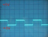
This is the BCK signal measured on the tda pin2. I am using the mk8 reclocker design... Is this normal behavior given the internal capacitance of the tda and limiting resistors? The WS trace is clear square wave with slight overshoot
Last edited:
So I designed a new masterclock. The design was optimized for lowest possible impact of power supply fluctuations and loading. By reducing the impact of external factors like power supply and load fluctuations, lower jitter is achieved under similar conditions.
The balanced masterclock was based on low noise RF JFETs. This design showed approx. 500Hz / volt frequency shift, similar as with conventional Collpitts and Pierce oscillators. The main reason for this is varying signal amplitude. So the next logical step was amplitude stabilization. This reduced frequency shift to 10Hz / volt typical.
Next problem is clock loading, any (capacitive) load on the oscillator output will shift oscillator frequency substantially. If the load capacitance changes (dynamically) it will modulate masterclock frequency with up to 10Hz / pF load change. By reducing clock load, the max. load induced frequency shift could be reduced. By using exactly the same load on both outputs and taking advantage of the balanced circuit the frequency shift could be minimized.
Then there is trigger uncertainty. Fluctuations in power supply will also change exact moment of triggering of the connected load. One solution is using a high speed comparator, but these have a certain hysteresis. This means there is a certain "dead zone" where the comparator doesn't respond (output is undefined). This means that the output signal phase can still vary within the hysteresis window.
I ended up using a "see-saw" circuit that is toggled alternatively by both masterclock outputs. If one output is earlier due to power supply rise, same will happen with the other output and the change is canceled as the time between toggling is kept virtually constant. The see-saw circuit also acts as clock buffer.
...
This new timing module offered the most substantial improvements in sound quality I ever achieved with my audio set.
John, can you share a bit more on the clock circuit you are using?
Hi studiostevus,
Grundig player has 4 x oversampling so both, WS and DEM clock equal 4 * 44.1 = 176.4 KHz vs 2.8224 MHz.
DEM clok rate would then have been 44,100 * 4 * 32 = 5.6448 MHz.
These are pre-regulators and are only part of the complete power supply. Their task is attenuating ripple voltage in order to get a clean DC voltage for the attached voltage regulator.
In the SD8 player I use a combination of cascaded capacitance multipliers (output ripple below 1mVpp), followed by 4th order balanced RC low pass and local shunt regulators. I also replaced all higher value ceramic caps with SMD film caps because there were problems with piezoelectric effects.
I attached an oscillogram of BCK signal (pin 2) measured on an earlier design (2010)
You need a large bandwidth scope of say 100MHz, suitable probes and have to remove the ground lead and use an adapter tip with short ground connection:
3GHz RF Probe
Grundig player has 4 x oversampling so both, WS and DEM clock equal 4 * 44.1 = 176.4 KHz vs 2.8224 MHz.
Makes you wonder why grundig didnt go for synchronization via bck
DEM clok rate would then have been 44,100 * 4 * 32 = 5.6448 MHz.
Now I am using the #4008 regulators with MODPWR2 preregulators, and I notice a significant detoriation in instrument separation, less clear highs, air, etc.
These are pre-regulators and are only part of the complete power supply. Their task is attenuating ripple voltage in order to get a clean DC voltage for the attached voltage regulator.
In the SD8 player I use a combination of cascaded capacitance multipliers (output ripple below 1mVpp), followed by 4th order balanced RC low pass and local shunt regulators. I also replaced all higher value ceramic caps with SMD film caps because there were problems with piezoelectric effects.
This is the BCK signal measured on the tda pin2.
I attached an oscillogram of BCK signal (pin 2) measured on an earlier design (2010)
You need a large bandwidth scope of say 100MHz, suitable probes and have to remove the ground lead and use an adapter tip with short ground connection:
3GHz RF Probe
Attachments
Hi studiostevus,
These are pre-regulators and are only part of the complete power supply. Their task is attenuating ripple voltage in order to get a clean DC voltage for the attached voltage regulator.
Hi John,
Sorry I was not clear: I meant I have built the MODPWR2 pre-regulators, followed by the mk8 post-regulators of post #4008. As mentioned, they are a step back compared to Salas regs. Frankly, my current setup hardly beats an unmodded philips cd-880.
You have moved on from those as well, and I see now why. No criticism here, just reporting my experiences
I attached an oscillogram of BCK signal (pin 2) measured on an earlier design (2010)
ion:
3GHz RF Probe
Reading back a couple of months, I see that you have lowered the voltage of the reclocker, which makes current limiting resistors on BCK unnecessary. That explains why you have a nice square
. Why do you still place current limiting resistors on WS and DATA (even though the SD transport outputs suitably levelled signals. I will use level translators to 1.8V to interface with my squeezebox myself) ?Also, I am very interested in understanding your clock design.
Last edited:
Hi studiostevus,
The problem is caused by the series voltage regulators that turned out to be less suitable for this application.
The TDA1541A-MK11 runs on shunt voltage regulators.
I experimented with many different CCS. They offer some noise / ripple rejection, but a single capacitance multiplier turned out to be much more effective in attenuating rectifier ripple / noise.
So I used two cascaded capacitance multipliers to attenuate rectifier ripple / noise. But since transistors aren't perfect either (they pass higher frequency noise through stray capacitance between collector and emitter), I added a 4th order balanced passive RC filter to tackle this noise. This balanced RC filter contains resistors that also provide required current limiting for the shunt regulators.
I use LED reference voltage as these offer lower noise compared to most zener diodes and (bandgap) voltage references. The LED voltage references are also bypassed with 220uF caps in order to further attenuate noise.
There is no reclocker in the new design, just a divider (divide-by-4) between masterclock and BCK. The divider output connects directly to BCK (no series resistors).
The masterclock runs on 3.6V, the clock buffer for the driving the external digital audio source runs on 3V. The divide-by-4 circuit runs on 1.8V.
The nice square was measured on a resistive BCK divider (330R / 1K) in 2010. The divide-by-4 circuit (2012) provides much steeper transients. BCK now has 1.8Vpp amplitude (no DC bias voltage).
SD8 transport outputs 3.3Vpp. These signals are attenuated and a bias voltage is added for minimum switching noise injection through ground-bounce. The resistors reduce WS and DATA signal bandwidth and attenuate the signal amplitude, both lead to reduced ground-bounce in the TDA1541A I2S input circuit.
The TDA1541A-MK11 module runs on two synchronized JFET Colpitts oscillators that share one 11.2896 MHz crystal. One output drives the BCK divider, the other drives the digital audio source through a clock buffer.
As mentioned, they are a step back compared to Salas regs.
The problem is caused by the series voltage regulators that turned out to be less suitable for this application.
The TDA1541A-MK11 runs on shunt voltage regulators.
I experimented with many different CCS. They offer some noise / ripple rejection, but a single capacitance multiplier turned out to be much more effective in attenuating rectifier ripple / noise.
So I used two cascaded capacitance multipliers to attenuate rectifier ripple / noise. But since transistors aren't perfect either (they pass higher frequency noise through stray capacitance between collector and emitter), I added a 4th order balanced passive RC filter to tackle this noise. This balanced RC filter contains resistors that also provide required current limiting for the shunt regulators.
I use LED reference voltage as these offer lower noise compared to most zener diodes and (bandgap) voltage references. The LED voltage references are also bypassed with 220uF caps in order to further attenuate noise.
I see that you have lowered the voltage of the reclocker
There is no reclocker in the new design, just a divider (divide-by-4) between masterclock and BCK. The divider output connects directly to BCK (no series resistors).
The masterclock runs on 3.6V, the clock buffer for the driving the external digital audio source runs on 3V. The divide-by-4 circuit runs on 1.8V.
That explains why you have a nice square
The nice square was measured on a resistive BCK divider (330R / 1K) in 2010. The divide-by-4 circuit (2012) provides much steeper transients. BCK now has 1.8Vpp amplitude (no DC bias voltage).
Why do you still place current limiting resistors on WS and DATA (even though the SD transport outputs suitably levelled signals.
SD8 transport outputs 3.3Vpp. These signals are attenuated and a bias voltage is added for minimum switching noise injection through ground-bounce. The resistors reduce WS and DATA signal bandwidth and attenuate the signal amplitude, both lead to reduced ground-bounce in the TDA1541A I2S input circuit.
Also, I am very interested in understanding your clock design.
The TDA1541A-MK11 module runs on two synchronized JFET Colpitts oscillators that share one 11.2896 MHz crystal. One output drives the BCK divider, the other drives the digital audio source through a clock buffer.
Hi Galeb,
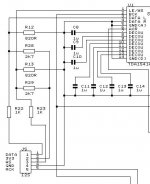
I attached the I2S attenuator / bias circuit for WS and DATA.
Input signal amplitude equals 3.3Vpp. Resistor of 1K is placed in series with the signal (R22, R23).
Resistor of 820R to GND and 2K7 to 3.3V power supply provide the bias voltage and together with the 1K series resistor they provide required signal attenuation.
The circuit provides approx. 1.76Vpp and a bias voltage of 1.115V.
hi john, could you post the signal conditioning schematic?
I attached the I2S attenuator / bias circuit for WS and DATA.
Input signal amplitude equals 3.3Vpp. Resistor of 1K is placed in series with the signal (R22, R23).
Resistor of 820R to GND and 2K7 to 3.3V power supply provide the bias voltage and together with the 1K series resistor they provide required signal attenuation.
The circuit provides approx. 1.76Vpp and a bias voltage of 1.115V.
Attachments
Hi EC,
in case of a classic Marantz/Philips CD Player what would be the value of the I2S input signal ? so I would like to know in accordance with this value the aprox. values of the resistors for the I2S attenuator - because I believe that your SD Card transport offers other/custom signal amplitude for the I2S signal compared to a readily available CD player , so these resistor values from your schematic would not be compatible for us who are modding our cd players using your advices;
Thanks
Hi luxury54,
The resistor values for 5V TTL signal levels of WS and DATA would be approx. 2K series resistor, 680R to ground and 5K6 to +5V. BCK is problematic, perhaps an ultra high speed level translator or divider / level translator could be used here.
In case of a classic Marantz/Philips CD Player what would be the value of the I2S input signal ?
The resistor values for 5V TTL signal levels of WS and DATA would be approx. 2K series resistor, 680R to ground and 5K6 to +5V. BCK is problematic, perhaps an ultra high speed level translator or divider / level translator could be used here.
- Home
- Source & Line
- Digital Line Level
- Building the ultimate NOS DAC using TDA1541A