Everyone has there favorites to work with which is great as long as they aren't PWM's ") . For exampe The PCM1704 sounds and measures good with 60-100 ohm passive I/V and post amplification, as long as you slow down the servo crap with over sized capacitors on the pins.
. For exampe The PCM1704 sounds and measures good with 60-100 ohm passive I/V and post amplification, as long as you slow down the servo crap with over sized capacitors on the pins.
Nothing wrong with the PCM56 or the TDA1541 either. Anything is better than the sigma-delta RFI generators.
My only issue was when we weren't working on a D/AC in this thread, rather a SD player permanately attached to a TDA1541 so it wasn't really functioning as a DAC since it was tied to sharing the clock with the specialized transport. The latest iteration that allows a smart method to download files to the memory card is a big step toward the title or scope of the thread.
I would like to hear Benard's DAC, but buying 32 PCM56 chips seems a bit impractical. So my interest is TDA1541, AD1862, PCM63, and PCM1704. All good chips and better than the modulators.
. For exampe The PCM1704 sounds and measures good with 60-100 ohm passive I/V and post amplification, as long as you slow down the servo crap with over sized capacitors on the pins.Nothing wrong with the PCM56 or the TDA1541 either. Anything is better than the sigma-delta RFI generators.
My only issue was when we weren't working on a D/AC in this thread, rather a SD player permanately attached to a TDA1541 so it wasn't really functioning as a DAC since it was tied to sharing the clock with the specialized transport. The latest iteration that allows a smart method to download files to the memory card is a big step toward the title or scope of the thread.
I would like to hear Benard's DAC, but buying 32 PCM56 chips seems a bit impractical. So my interest is TDA1541, AD1862, PCM63, and PCM1704. All good chips and better than the modulators.
Last edited:
Hi studiostevus,
The maximum regulator output current (capacitance multiplier) also depends on BD679 base current / Hfe.
When higher output current is desired you need to increase base current (decrease resistor value between base and collector).
This in turn will increase ripple voltage on the capacitor (capacitance multiplier), so a larger capacitor value is needed.
I use a 2A capacitance multiplier for the modified Circlotron output stage that runs on a single power supply.
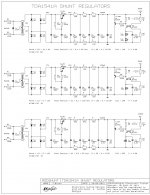
The latest power supplies consist of rectifier, capacitance multiplier, balanced passive RC filter and shunt regulator. This configuration offers very clean DC voltage even with highly polluted mains voltage (attached schematic).
There are some new developments with the TDA1541A-MK10. When using high resolution amplifier and speakers there were some slight problems with upper midrange and trebles that were traced down to the current buffer circuit.
In order to find a solution I tested most basic I/V conversion, resistor between DAC output and ground.The 2mA bias current (TDA1541A) creates an unwanted DC voltage on the DAC output. With say 39 Ohms passive I/V resistor we get 0.002 (bias current) * 39 = -78mV DC while the ac voltage equals 0.004 (full-scale) * 39 = 156mVpp. This means that the signal varies between -156mVpp and 0V instead of +78 and -78mV as desired.
So I added a compensation current by connecting approx. 2K5 resistor between +5V and DAC output. Now the signal swings between +78 and -78mV and DC at the DAC output is around zero. The compensation current now varies between (5-0.078) / 2500 = +1.96mA and (5+0.078) / 2500 = +2.03mA.
I was able to generate up to 500mVpp with low distortion using 2K5 and 120 Ohms. The issues with upper midrange and trebles were now gone.
In order to amplify the signal I was thinking of using an Aikido JFET or tube amplifier. Some tests with a 2SK389-based Aikido JFET amplifier gave good results.
There is also an interesting Aikido LV kit that runs on a single 24 or 48 volt DC supply (heaters included):
Aikido LV.
The maximum regulator output current (capacitance multiplier) also depends on BD679 base current / Hfe.
When higher output current is desired you need to increase base current (decrease resistor value between base and collector).
This in turn will increase ripple voltage on the capacitor (capacitance multiplier), so a larger capacitor value is needed.
I use a 2A capacitance multiplier for the modified Circlotron output stage that runs on a single power supply.
The latest power supplies consist of rectifier, capacitance multiplier, balanced passive RC filter and shunt regulator. This configuration offers very clean DC voltage even with highly polluted mains voltage (attached schematic).
There are some new developments with the TDA1541A-MK10. When using high resolution amplifier and speakers there were some slight problems with upper midrange and trebles that were traced down to the current buffer circuit.
In order to find a solution I tested most basic I/V conversion, resistor between DAC output and ground.The 2mA bias current (TDA1541A) creates an unwanted DC voltage on the DAC output. With say 39 Ohms passive I/V resistor we get 0.002 (bias current) * 39 = -78mV DC while the ac voltage equals 0.004 (full-scale) * 39 = 156mVpp. This means that the signal varies between -156mVpp and 0V instead of +78 and -78mV as desired.
So I added a compensation current by connecting approx. 2K5 resistor between +5V and DAC output. Now the signal swings between +78 and -78mV and DC at the DAC output is around zero. The compensation current now varies between (5-0.078) / 2500 = +1.96mA and (5+0.078) / 2500 = +2.03mA.
I was able to generate up to 500mVpp with low distortion using 2K5 and 120 Ohms. The issues with upper midrange and trebles were now gone.
In order to amplify the signal I was thinking of using an Aikido JFET or tube amplifier. Some tests with a 2SK389-based Aikido JFET amplifier gave good results.
There is also an interesting Aikido LV kit that runs on a single 24 or 48 volt DC supply (heaters included):
Aikido LV.
Attachments
Last edited:
John, if you use 120 ohms passive I/V resistor, you have +240mV and -240mV. This is OK for the audio output level, but you far exceed the +/-25mV voltage compliance of the TDA1541A. As I remember, there are some internal diodes that get forward biased and cause distortion above that level (although it is most likely not a hard limit). Have you taken any special measures to avoid this distortion?In order to find a solution I tested most basic I/V conversion, resistor between DAC output and ground.The 2mA bias current (TDA1541A) creates an unwanted DC voltage on the DAC output. With say 39 Ohms passive I/V resistor we get 0.002 (bias current) * 39 = -78mV DC while the ac voltage equals 0.004 (full-scale) * 39 = 156mVpp. This means that the signal varies between -156mVpp and 0V instead of +78 and -78mV as desired.
So I added a compensation current by connecting approx. 2K5 resistor between +5V and DAC output. Now the signal swings between +78 and -78mV and DC at the DAC output is around zero. The compensation current now varies between (5-0.078) / 2500 = +1.96mA and (5+0.078) / 2500 = +2.03mA.
I was able to generate up to 500mVpp with low distortion using 2K5 and 120 Ohms.
Dear ec
Still I have to answer your last post...
To this one:
You could not hear the problems before ?
Don't you think that a 2,5k resistor will inject noise into the circuit ?
Did you measure the distortion with decent equipment or did you look at the waveform with a scope ? Remember the 25mV voltage compliance.
Now post amplification ?
There are some new developments with the TDA1541A-MK10. When using high resolution amplifier and speakers there were some slight problems with upper midrange and trebles that were traced down to the current buffer.
So I added a compensation current by connecting approx. 2K5 resistor between +5V and DAC output. Now the signal swings between +78 and -78mV and DC at the DAC output is around zero. The compensation current now varies between (5-0.078) / 2500 = +1.96mA and (5+0.078) / 2500 = +2.03mA.
I was able to generate up to 500mVpp with low distortion using 2K5 and 120 Ohms. The issues with upper midrange and trebles were now gone.
In order to amplify the signal I was thinking of using an Aikido JFET or tube amplifier. Some tests with a 2SK389-based Aikido JFET amplifier gave good results.
Still I have to answer your last post...
To this one:
You could not hear the problems before ?
Don't you think that a 2,5k resistor will inject noise into the circuit ?
Did you measure the distortion with decent equipment or did you look at the waveform with a scope ? Remember the 25mV voltage compliance.
Now post amplification ?
Last edited:
ThorstenL
Would it be big trouble for you to post -60dB FFT ?
A number of parameters, including 0dBfs and -60dBfs FFT.
Would it be big trouble for you to post -60dB FFT ?
Hi Bernhard,
No, the performance of my audio set gradually improved and these marginal distortions became more clearly audible after these improvements.
The distortion is mainly audible on specific vocals on some audiophile recordings like from Stockfish.
Yes it will, but it also depends on power supply noise levels. The power supplies in the latest MK10 (schematics in my previous post) are very clean, and I applied additional RC filtering between 5V supply and bias resistor.
Of course I also tested (JFET) CCS. This resulted in slight grain and more agressive upper midrange and trebles. So it basically re-introduced some of the problems I experienced with the current buffer circuit.
Yes I did, Marconi TF2331A distortion meter indicates approx. 0.02% THD + noise (DAC + Aikido line amplifier). The TF2331 also has an output (extracted THD + noise). This output signal can be used to analyse the distortion + noise.
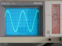
The first oscillogram shows the 1 KHz output signal (3Vpp) at the Aikido line amplifier output. Voltage across the 120R passive I/V resistor equals 480mVpp and positive bias current equals 2mA.
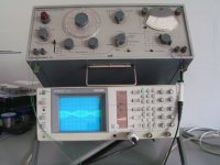
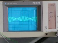
The second picture shows THD measurement setup. The TF2331A indicates approx. 0.02% THD & noise. The scope shows the distortion meter output signal. The distortion mainly consists of quantization noise as can be seen on the oscillogram.
When using oversampling / reconstruction filtering the quantization noise can be significantly reduced and THD + noise can be lowered to approx. 0.002%.
The DACs presented at the beginning of this thread did just that, significantly reducing quantization noise and thus reducing THD for bass-midrange. Since the midrange is very important for audio this wasn't such a bad idea after all.
It is obvious that linear interpolation causes increased THD at higher frequencies as you already pointed out. So why not use the best of both worlds, linear interpolation (4 ... 8 DAC chips in parallel) for bass / midrange and a second NOS DAC just for upper midrange and trebles?
When using a 2-way speaker each DAC could drive a dedicated speaker chassis, filtered interpolation DAC feeds bass / midrange chassis and filtered / corrected NOS DAC drives the tweeter chassis. Trebles boost can be used for the tweeter only in order to compensate for trebles roll-off without affecting bass-midrange. The delay circuits (shift registers) can be used to time-align both OS and NOS DAC output signals.
You could not hear the problems before ?
No, the performance of my audio set gradually improved and these marginal distortions became more clearly audible after these improvements.
The distortion is mainly audible on specific vocals on some audiophile recordings like from Stockfish.
Don't you think that a 2,5k resistor will inject noise into the circuit ?
Yes it will, but it also depends on power supply noise levels. The power supplies in the latest MK10 (schematics in my previous post) are very clean, and I applied additional RC filtering between 5V supply and bias resistor.
Of course I also tested (JFET) CCS. This resulted in slight grain and more agressive upper midrange and trebles. So it basically re-introduced some of the problems I experienced with the current buffer circuit.
Did you measure the distortion with decent equipment or did you look at the waveform with a scope ? Remember the 25mV voltage compliance.
Yes I did, Marconi TF2331A distortion meter indicates approx. 0.02% THD + noise (DAC + Aikido line amplifier). The TF2331 also has an output (extracted THD + noise). This output signal can be used to analyse the distortion + noise.
The first oscillogram shows the 1 KHz output signal (3Vpp) at the Aikido line amplifier output. Voltage across the 120R passive I/V resistor equals 480mVpp and positive bias current equals 2mA.
The second picture shows THD measurement setup. The TF2331A indicates approx. 0.02% THD & noise. The scope shows the distortion meter output signal. The distortion mainly consists of quantization noise as can be seen on the oscillogram.
When using oversampling / reconstruction filtering the quantization noise can be significantly reduced and THD + noise can be lowered to approx. 0.002%.
The DACs presented at the beginning of this thread did just that, significantly reducing quantization noise and thus reducing THD for bass-midrange. Since the midrange is very important for audio this wasn't such a bad idea after all.
It is obvious that linear interpolation causes increased THD at higher frequencies as you already pointed out. So why not use the best of both worlds, linear interpolation (4 ... 8 DAC chips in parallel) for bass / midrange and a second NOS DAC just for upper midrange and trebles?
When using a 2-way speaker each DAC could drive a dedicated speaker chassis, filtered interpolation DAC feeds bass / midrange chassis and filtered / corrected NOS DAC drives the tweeter chassis. Trebles boost can be used for the tweeter only in order to compensate for trebles roll-off without affecting bass-midrange. The delay circuits (shift registers) can be used to time-align both OS and NOS DAC output signals.
Attachments
Last edited:
Can you post some more info and maybe a schema of this Circlotron?I use a 2A capacitance multiplier for the modified Circlotron output stage that runs on a single power supply.
This would be much appreciated
When using oversampling / reconstruction filtering the quantization noise can be significantly reduced and THD + noise can be lowered to approx. 0.002%.
The DACs presented at the beginning of this thread did just that, significantly reducing quantization noise and thus reducing THD for bass-midrange. Since the midrange is very important for audio this wasn't such a bad idea after all.
It is obvious that linear interpolation causes increased THD at higher frequencies as you already pointed out. So why not use the best of both worlds, linear interpolation (4 ... 8 DAC chips in parallel) for bass / midrange and a second NOS DAC just for upper midrange and trebles?
Hello John
Most of the signals for the imaging/soundstage and engagement in a music recording are roughly between 2 Khz and 6 Khz
Using linear interpolation could be good in that frequencies range, but at
6 Khz linear interpolation start to have higher THD
Up to which frequencies you whould use linear interpolation ?
Thank
Bye
Gaetan
Last edited:
John:
this IS getting interesting!
So why not use the best of both worlds, linear interpolation (4 ... 8 DAC chips in parallel) for bass / midrange and a second NOS DAC just for upper midrange and trebles?
Hello John
Most of the signals for the imaging/soundstage and engagement in a music recording are roughly between 2 Khz and 6 Khz
Using linear interpolation could be good in that frequencies range, but at
6 Khz linear interpolation start to have higher THD
this IS getting interesting!
Most of the signals for the imaging/soundstage and engagement in a music recording are roughly between 2 Khz and 6 Khz
Is that science?
My personal experience is that the most important area of audio lies within the 'voice' range 200hz<>3khz
To add to the debate of Crossover Frequency Selection.
Here he talks about what he calls the musics "intelligence band" of 300Hz to 3600Hz
BiAmp (Bi-Amplification - Not Quite Magic, But Close) - Part 2
Here he talks about what he calls the musics "intelligence band" of 300Hz to 3600Hz
BiAmp (Bi-Amplification - Not Quite Magic, But Close) - Part 2
New developments,
This week I completed some TDA1541A-MK11 modules. After performing tests with passive I/V conversion using 120R from TDA1541A to GND and 2mA bias current to +5V it turned out this resulted in limited dynamics and caused some other problems like the need for extra amplification.
The MK11 I/V stage is based on a RF JFET cascode current buffer connected between TDA1541A output and a 7mA RF JFET CCS that connects to +5V. Resistor or CCS from TDA1541A output to GND provides a 3mA bias current for the current buffer.
Both, DAC output current and 3mA bias current are subtracted from the 7mA CCS and the remaining current flows through a 500R Rhopoint wire-wound I/V resistor that connects to GND. This offers 2Vpp as before. The bandwidth of this circuit is almost equal to RF JFET FT (700 MHz). So it's important to use short wiring and un-interrupted ground plane.
There are two trimmers on the current buffers for L/R channel DC offset at the TDA1541A outputs.
The reference voltage for DC-coupling now equals around +1.6V and can be decoupled to GND instead of +5V. This prevents external interference being dumped on the +5V supply. An additional trimmer is provided to set this reference voltage.
The TDA1541A-MK11 runs on the proven masterclock / clock buffer and synchronous BCK divider circuits. DEM soft sync circuit offers best DEM circuit operation so far.
Active divider decoupling is located underneath the TDA1541A and consists of 1uF 1210 size SMD film caps. The TDA 1541A is placed in an IC socket and there are no parts soldered to this chip so it can be swapped easily.
Resistive I2S attenuators are used for WS and DATA signals. The MK11 outputs 11.2896 MHz for slaving external sources.
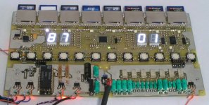
The stepped shunt volume control based on Rhoint resistors and sub miniature signal relays works fine. It is controlled through a serial interface that connects to the SD8 transport. The attenuation is displayed on the 7 segments displays during volume change. It is soldered directly to the DAC for minimum (capacitive) losses between DAC and volume control.
I attached a photograph of SD8-transport, MK11 DAC and stepped shunt volume control while being tested.
This week I completed some TDA1541A-MK11 modules. After performing tests with passive I/V conversion using 120R from TDA1541A to GND and 2mA bias current to +5V it turned out this resulted in limited dynamics and caused some other problems like the need for extra amplification.
The MK11 I/V stage is based on a RF JFET cascode current buffer connected between TDA1541A output and a 7mA RF JFET CCS that connects to +5V. Resistor or CCS from TDA1541A output to GND provides a 3mA bias current for the current buffer.
Both, DAC output current and 3mA bias current are subtracted from the 7mA CCS and the remaining current flows through a 500R Rhopoint wire-wound I/V resistor that connects to GND. This offers 2Vpp as before. The bandwidth of this circuit is almost equal to RF JFET FT (700 MHz). So it's important to use short wiring and un-interrupted ground plane.
There are two trimmers on the current buffers for L/R channel DC offset at the TDA1541A outputs.
The reference voltage for DC-coupling now equals around +1.6V and can be decoupled to GND instead of +5V. This prevents external interference being dumped on the +5V supply. An additional trimmer is provided to set this reference voltage.
The TDA1541A-MK11 runs on the proven masterclock / clock buffer and synchronous BCK divider circuits. DEM soft sync circuit offers best DEM circuit operation so far.
Active divider decoupling is located underneath the TDA1541A and consists of 1uF 1210 size SMD film caps. The TDA 1541A is placed in an IC socket and there are no parts soldered to this chip so it can be swapped easily.
Resistive I2S attenuators are used for WS and DATA signals. The MK11 outputs 11.2896 MHz for slaving external sources.
The stepped shunt volume control based on Rhoint resistors and sub miniature signal relays works fine. It is controlled through a serial interface that connects to the SD8 transport. The attenuation is displayed on the 7 segments displays during volume change. It is soldered directly to the DAC for minimum (capacitive) losses between DAC and volume control.
I attached a photograph of SD8-transport, MK11 DAC and stepped shunt volume control while being tested.
Attachments
Hello John,
I understood your your MK11 current buffer in principle but not in detail:
The reference voltage is about 1.6V. I suppose this voltage is across the 500R resistor if
the TDA1541A provides no AC signal. The current through the resistor is 3.2mA.
The remaining current through the JFET is 3.8mA (7mA-3.2mA)
Is it correct that that resistor/CCS for the 3mA buffer bias current is connected to GND
(and not to -15V) since the TDA1541A output is adjusted near to 0V.
How is the interaction between the 3mA resistor/CCS and the TDA1541A internal current
source which is 2mA with no AC signal.
Can you post a schematic for better understanding?
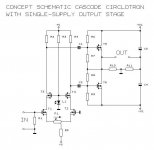
Hi marconi118,
I attached a concept schematic of the Ciclotron. The Circlotron output stage runs on a single power supply instead of two isolated power supplies. The circuit is still a parallel push-pull concept like the Circlotron.
The differential cascode input / driver stage / phase splitter runs on a separate high voltage supply (80 ... 120V) in order to maximize headroom, eliminate interference from the output stage, and achieve fairly constant current through R5.
Bias current equals approx. 2 x 10mA. Input is DC-coupled. LED L1 provides bias voltage for the cascode (T3, T4).
Output stage consists of T5 and T6. Each MOSFET has a separate bias circuit (R6. R7, T5 and R8, R9, T6). Bias current is set to approx. 400 ... 500mA (no signal).
R10 and R11 create required reference for signal injection (C1, C2).
Signal path T5: C1, gate, source, R10, ground.
Signal path T6: C2, gate, source, C4, R11, ground.
Asuming C3 and C4 are short circuit for ac signals, signal path for T6 can be viewed as:
C2, gate, source, R11, ground.
Can you post some more info and maybe a schema of this Circlotron? This would be much appreciated
I attached a concept schematic of the Ciclotron. The Circlotron output stage runs on a single power supply instead of two isolated power supplies. The circuit is still a parallel push-pull concept like the Circlotron.
The differential cascode input / driver stage / phase splitter runs on a separate high voltage supply (80 ... 120V) in order to maximize headroom, eliminate interference from the output stage, and achieve fairly constant current through R5.
Bias current equals approx. 2 x 10mA. Input is DC-coupled. LED L1 provides bias voltage for the cascode (T3, T4).
Output stage consists of T5 and T6. Each MOSFET has a separate bias circuit (R6. R7, T5 and R8, R9, T6). Bias current is set to approx. 400 ... 500mA (no signal).
R10 and R11 create required reference for signal injection (C1, C2).
Signal path T5: C1, gate, source, R10, ground.
Signal path T6: C2, gate, source, C4, R11, ground.
Asuming C3 and C4 are short circuit for ac signals, signal path for T6 can be viewed as:
C2, gate, source, R11, ground.
Attachments
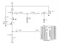
Hi JOSI1,
I attached I/V stage concept schematics.
With no signal TDA1541A outputs 2mA bias current. This current varies between 0 and 4mA with input signal.
No signal: current through R3 equals 7.5mA (CCS) - 2mA (DAC) - 2.7mA (R2) = 2.8mA. This gives 0.0028 * 500 = +1.4V DC.
DAC output 0 mA: current through R3 equals 7.5mA (CCS) - 0mA (DAC) - 2.7mA (R2) = 4.8mA. This gives 0.0048 * 500 = +2.4V
DAC output 4 mA: current through R3 equals 7.5mA (CCS) - 4mA (DAC) - 2.7mA (R2) = 0.8mA. This gives 0.0008 * 500 = +0.4V
So signal amplitude across R3 equals 2.4V - 0.4V = 2Vpp.
DC voltage at DAC output is set @ 0V with trimmer P1.
Note that there is always at least 2.7mA bias current running through the cascoded current buffer (T1 & T2).
DC-coupled output is achieved with decoupled adjustable reference voltage (P2). P2 is trimmed to match DC voltage across R3, in this example +1.4V.
This reference voltage is decoupled to GND and serves as reference for connected (pre) amplifiers. The circuit GND is -not- connected to external equiplent.
This circuit offers improved dynamics, lower distortion and better transient impuls response compared to pure passive I/V conversion. There is also no need for extra amplification (and related bandwidth reduction).
I used low noise (0.5dB) RF JFETs with Ft of around 700MHz. So the I/V converter has very large bandwidth and good linearity (cascode).
The measured input impedance of the cascode current buffer equals approx. 60 Ohms.
I understood your your MK11 current buffer in principle but not in detail:
Can you post a schematic for better understanding?
I attached I/V stage concept schematics.
With no signal TDA1541A outputs 2mA bias current. This current varies between 0 and 4mA with input signal.
No signal: current through R3 equals 7.5mA (CCS) - 2mA (DAC) - 2.7mA (R2) = 2.8mA. This gives 0.0028 * 500 = +1.4V DC.
DAC output 0 mA: current through R3 equals 7.5mA (CCS) - 0mA (DAC) - 2.7mA (R2) = 4.8mA. This gives 0.0048 * 500 = +2.4V
DAC output 4 mA: current through R3 equals 7.5mA (CCS) - 4mA (DAC) - 2.7mA (R2) = 0.8mA. This gives 0.0008 * 500 = +0.4V
So signal amplitude across R3 equals 2.4V - 0.4V = 2Vpp.
DC voltage at DAC output is set @ 0V with trimmer P1.
Note that there is always at least 2.7mA bias current running through the cascoded current buffer (T1 & T2).
DC-coupled output is achieved with decoupled adjustable reference voltage (P2). P2 is trimmed to match DC voltage across R3, in this example +1.4V.
This reference voltage is decoupled to GND and serves as reference for connected (pre) amplifiers. The circuit GND is -not- connected to external equiplent.
This circuit offers improved dynamics, lower distortion and better transient impuls response compared to pure passive I/V conversion. There is also no need for extra amplification (and related bandwidth reduction).
I used low noise (0.5dB) RF JFETs with Ft of around 700MHz. So the I/V converter has very large bandwidth and good linearity (cascode).
The measured input impedance of the cascode current buffer equals approx. 60 Ohms.
Attachments
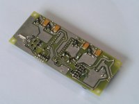
TDA1541A-Mk11 pictures
I attached some pictures of the latest TDA1541A-MK11 DAC.
First picture shows the component side. SMD film decoupling caps are located on the PCB, underneath the TDA1541A. The TDA1541A can be swapped easily (socket).
Film capacitors were used where possible in order to eliminate unwanted piezoelectric effects of ceramic caps. Only exception are the low value NPO caps (8.2pF ... 33pF).
There are 4 discrete shunt regulators, 3V6, -5V, -15V, +5 (left to right). Circuit is designed so transistor heatsink (collector) can be soldered to the ground plane for optimal cooling.
The two transparent trimmers are for 0V DC adjustment (L+R) on the TDA1541A outputs.
The black trimmer (bottom right) is used for DC-reference voltage. The electrolytic cap above it decouples DC reference voltage to GND.
I/V resistors are 500R 0.1% Rhopoint non-inductive wirewound.
Second picture shows the solder side. Masterclock is on the bottom left. It consist of two synchronized oscillators. Miniature crystal is used. Clock buffer and BCK divide-by-4 circuit are located very close to the masterclock. The divider output in turn is located very close to the TDA1541A BCK input (pin2). Buffered 11.2896 MHz output is provided for slaving digital audio sources (leftmost pin on the I2S connector).
The resistive I2S attenuators are located close to the I2S connector. Again I2S signal path is kept very short by placing the I2S connector close to the TDA1541A. Note that the MK11 only requires WS and DATA, BCK is provided by the divide-by-4 circuit.
The I/V circuits (bottom right) consist of cascoded current buffers and JFET CCS. There are 6 JFETs in total.
The discrete shunt voltage regulators are located at the top. LED reference is decoupled by a 220uF tantalum capacitor. These regulators require external current limiting (resistors). Power supply wiring needs to be shielded.
Attachments
Member
Joined 2006
Hi John,
If I see correctly, you are currently only using 1 DEM reclocking line (I guess synchronized and attenuated BCK). What triggered this change? Is the other pin now left floating?
Also WS and DATA seem to be straight from the source module, without additional reclocking via MCLK/BCK. Does this reduce jitter compared to reclocking based on MCLK/BCK? I guess you completely rely then on edge-triggering inside the TDA?
- Home
- Source & Line
- Digital Line Level
- Building the ultimate NOS DAC using TDA1541A