Hi bernhard,
The graphite compound may have RF absorbing properties, some RF absorbing foams are based on carbon:
Graphite - Wikipedia, the free encyclopedia
RF and Microwave Absorber - Ferrite Tiles and Foam Absorber
RF Absorbing Material
RF Microwave Absorbers| ETS-Lindgren
Above materials are described as microwave absorbers. Modern wireless communication devices use and generate frequencies in the microwave spectrum.
Altmann already indicates that the graphite compound is intended to attenuate higher harmonics.
Here is an example of a practical application of such RF absorbing foam in a masterclock:
NewClassD Neutron Star
A much better and well proofed solution is angel dust scattered all over the pcb.
The graphite compound may have RF absorbing properties, some RF absorbing foams are based on carbon:
Graphite - Wikipedia, the free encyclopedia
RF and Microwave Absorber - Ferrite Tiles and Foam Absorber
RF Absorbing Material
RF Microwave Absorbers| ETS-Lindgren
Above materials are described as microwave absorbers. Modern wireless communication devices use and generate frequencies in the microwave spectrum.
Altmann already indicates that the graphite compound is intended to attenuate higher harmonics.
Here is an example of a practical application of such RF absorbing foam in a masterclock:
NewClassD Neutron Star
Hi Sandor,
The measured output impedance of my Circlotron monoblocks equals approx. 0.4 Ohms and I run them with 8 Ohm load.
When using 2 Ohm loads, efficiency will drop. Speaker interlinks and connections could also become more problematic (increased voltage drop caused by increased currents).
The circlotrons remain fully stable, even when output is short-circuit or the speakers are connected / disconnected during operation.
One could experiment with different power MOSFETs in the output stage in order to lower output impedance if required.
Hello John,
how does your circlotron amp perform with loads as low as 2 ohms?
The measured output impedance of my Circlotron monoblocks equals approx. 0.4 Ohms and I run them with 8 Ohm load.
When using 2 Ohm loads, efficiency will drop. Speaker interlinks and connections could also become more problematic (increased voltage drop caused by increased currents).
The circlotrons remain fully stable, even when output is short-circuit or the speakers are connected / disconnected during operation.
One could experiment with different power MOSFETs in the output stage in order to lower output impedance if required.
Hello ecdesigns,
You Circlotron amp looks very interesting and full of knowledge. I would like to build them to use on my speakers and would like to ask some question.
How to connect to input on your Circlotron amp circuit? Cap input on both input and ground? Or just cap input.
2sj79 is also hard to find. Is there an alternative part?
On your "hybridge smoothing cap", seem like you use small parallel cap instead of one big cap. Is there a guide on how to choose and combine cap? For example, if I want to use 22,000uF cap, how to choose small combine caps? (4,700UF + 3,300uF + 2,200uF + 2200uF )x2 ?
Thanks for sharing your knowledge.
Hi WT,
I can only advice not to use any coupling caps, anywhere in the signal path. Even the very best distort, add coloration and reduce resolution and speed. This sound coloration can produce an "impressive" or warm sound with lots of "air", but the sound won't be transparent as it is simply distorted by adding harmonics that weren't present in the original recording. The use of coupling caps also increases the risk of improving the sound of specific recording and degrading sound of others.
With a highly transparent (DC-coupled) set, all recordings sound at their very best and there is no preference for any type of music.
The Circlotron power amp is fully DC-coupled, so no coupling caps needed, provided input signal has low DC offset (few millivolts DC or less).
The schematic shows a single-ended input version.
It is possible to connect both P-MOSFET gates to GND using 100K resistor and use balanced interface. In this case the symmetry circuit consisting of R20 (12K) and C26 (4u7) can be removed as both P-MOSFETs now operate in grounded-source mode and thus have equal gain.
Other pats can be used, preferably lateral MOSFETs with high enough gain. Popular JFETs (2SJ109 / 2SJ74) sound grainy with less far less resolution by comparison. I suspect this has something to do with thermal memory effects.
Depending on MOSFET specs (gate threshold voltage) value of some parts like R15 may need to be changed. Remember that the differential input stage bias current (DC voltage drop across R18 and R19) directly affects Circlotron output stage bias current. In practice you either end up with too high bias current or no bias current at all. Also very important, both P-MOSFETS and both N-power MOSFETs need to be matched pairs.
Each capacitor has characteristic resonance spectrum. It is unlikely that resonance spectra of capacitors of different value or construction are exactly the same. By paralleling multiple "different" capacitors, resonance spectrum of one cap can be attenuated by another cap that's placed in parallel, and vice versa. The result is reduced resonance and reduced sound coloration as unwanted harmonics are being attenuated.
These resonances are audible when connecting a cap to a function generator and slowly sweep through the audio spectrum.
For 22,000uF cap you could approximate this value as closely as required using capacitors with different value (size) like 4700uF, 3300uF, 2200uF, 1000uF and so on.
With higher output power rating it is required to use suitable twisted pairs wire connection directly between smoothing cap bank and power MOSFET pins. This minimizes power interlink inductance and unwanted crosstalk.
How to connect to input on your Circlotron amp circuit? Cap input on both input and ground? Or just cap input.
I can only advice not to use any coupling caps, anywhere in the signal path. Even the very best distort, add coloration and reduce resolution and speed. This sound coloration can produce an "impressive" or warm sound with lots of "air", but the sound won't be transparent as it is simply distorted by adding harmonics that weren't present in the original recording. The use of coupling caps also increases the risk of improving the sound of specific recording and degrading sound of others.
With a highly transparent (DC-coupled) set, all recordings sound at their very best and there is no preference for any type of music.
The Circlotron power amp is fully DC-coupled, so no coupling caps needed, provided input signal has low DC offset (few millivolts DC or less).
The schematic shows a single-ended input version.
It is possible to connect both P-MOSFET gates to GND using 100K resistor and use balanced interface. In this case the symmetry circuit consisting of R20 (12K) and C26 (4u7) can be removed as both P-MOSFETs now operate in grounded-source mode and thus have equal gain.
2sj79 is also hard to find. Is there an alternative part?
Other pats can be used, preferably lateral MOSFETs with high enough gain. Popular JFETs (2SJ109 / 2SJ74) sound grainy with less far less resolution by comparison. I suspect this has something to do with thermal memory effects.
Depending on MOSFET specs (gate threshold voltage) value of some parts like R15 may need to be changed. Remember that the differential input stage bias current (DC voltage drop across R18 and R19) directly affects Circlotron output stage bias current. In practice you either end up with too high bias current or no bias current at all. Also very important, both P-MOSFETS and both N-power MOSFETs need to be matched pairs.
On your "hybridge smoothing cap", seem like you use small parallel cap instead of one big cap. Is there a guide on how to choose and combine cap? For example, if I want to use 22,000uF cap, how to choose small combine caps? (4,700UF + 3,300uF + 2,200uF + 2200uF )x2 ?
Each capacitor has characteristic resonance spectrum. It is unlikely that resonance spectra of capacitors of different value or construction are exactly the same. By paralleling multiple "different" capacitors, resonance spectrum of one cap can be attenuated by another cap that's placed in parallel, and vice versa. The result is reduced resonance and reduced sound coloration as unwanted harmonics are being attenuated.
These resonances are audible when connecting a cap to a function generator and slowly sweep through the audio spectrum.
For 22,000uF cap you could approximate this value as closely as required using capacitors with different value (size) like 4700uF, 3300uF, 2200uF, 1000uF and so on.
With higher output power rating it is required to use suitable twisted pairs wire connection directly between smoothing cap bank and power MOSFET pins. This minimizes power interlink inductance and unwanted crosstalk.
Hi WT,
This schematic is not fully correct, the 100K resistors should connect to +15V that serves as input signal reference, just like in the schematic I posted. This is required in order to maximize output signal amplitude of the combined differential input / driver stage.
In conventional designs the (differential) input stage is referenced to GND, but has limited output signal amplitude. The (differential) driver stage then amplifies this signal.
My first Circlotron prototype had a differential input stage that did have GND as reference, this input stage was connected to a driver stage that would provide required output signal amplitude to drive the power MOSFETs. Problem was increased distortion and loss of resolution caused by the two extra MOSFETs.
What I did was removing the differential input stage, and using the existing differential driver stage to serve as input stage as well. Since I needed full DC-coupling there was little other option than adding an extra +15V power supply for input / driver stage reference.
The Circlotron power amp is powered through a number of transformers, so the circuit basically "floats" as it isn't connected to any other circuits. Then one can use +15V as reference, provided one doesn't connect GND of the audio source with GND of Circlotron power amp. So the GND used in the Circlotron circuit is only used locally, and serves as reference for the power MOSFETs.
Just to make sure that I understand you correctly. For balance input circlotron, the schematic should look like this. Is it correct?
This schematic is not fully correct, the 100K resistors should connect to +15V that serves as input signal reference, just like in the schematic I posted. This is required in order to maximize output signal amplitude of the combined differential input / driver stage.
In conventional designs the (differential) input stage is referenced to GND, but has limited output signal amplitude. The (differential) driver stage then amplifies this signal.
My first Circlotron prototype had a differential input stage that did have GND as reference, this input stage was connected to a driver stage that would provide required output signal amplitude to drive the power MOSFETs. Problem was increased distortion and loss of resolution caused by the two extra MOSFETs.
What I did was removing the differential input stage, and using the existing differential driver stage to serve as input stage as well. Since I needed full DC-coupling there was little other option than adding an extra +15V power supply for input / driver stage reference.
The Circlotron power amp is powered through a number of transformers, so the circuit basically "floats" as it isn't connected to any other circuits. Then one can use +15V as reference, provided one doesn't connect GND of the audio source with GND of Circlotron power amp. So the GND used in the Circlotron circuit is only used locally, and serves as reference for the power MOSFETs.
This schematic is not fully correct, the 100K resistors should connect to +15V that serves as input signal reference, just like in the schematic I posted. This is required in order to maximize output signal amplitude of the combined differential input / driver stage./QUOTE]
Got this
One more question, Sorry if I ask too many questions. If I build the circlotron as stand alone amp, it will have 15 V at the input and ground input. What is your recommendation for connect it from pre-amp. Transformer coupling?
Hi WT,
There would be no ground input. Ground connections remain inside the monoblock housing. Signal reference and signal inputs will all be at same potential (+15V) with respect to the internal ground that is not present at any external terminal or metal housing. So one can simply imagine dealing with a plain differential input that can be connected like any other.
Pre-amps, (coupling) caps and (coupling) transformers in the signal path add clearly audible distortion / coloration and cause loss of resolution. So try not to use these in high performance audio equipment.
One more question, Sorry if I ask too many questions. If I build the circlotron as stand alone amp, it will have 15 V at the input and ground input. What is your recommendation for connect it from pre-amp. Transformer coupling?
There would be no ground input. Ground connections remain inside the monoblock housing. Signal reference and signal inputs will all be at same potential (+15V) with respect to the internal ground that is not present at any external terminal or metal housing. So one can simply imagine dealing with a plain differential input that can be connected like any other.
Pre-amps, (coupling) caps and (coupling) transformers in the signal path add clearly audible distortion / coloration and cause loss of resolution. So try not to use these in high performance audio equipment.
Does this TDA1541 reclock and dem clock circuit would work good ?
The I2S attenuators aren't optimal, better use new I2S attenuator circuits from the TDA1541A-MK6. failing to use suitable I2S attenuators will lead to higher on-chip ground-bounce and resulting higher on-chip jitter levels.
Here are calculated max! jitter levels for 44.1/16 NOS with indicated resolution:
44.1/16 NOS, 0.1 LSB (15.5 bit resolution), 1 / (44,100 * 1) / (2^16 / (1 / 0.5)) = 173ps.
44.1/16 NOS, 0.1 LSB (15.9 bit resolution), 1 / (44,100 * 1) / (2^16 / (1 / 0.1)) = 34.6ps.
44.1/16 NOS, 0.01 LSB (15.99 bit resolution),1 / (44,100 * 1) / (2^16 / (1 / 0.01)) = 3.46ps.
Jitter specs get even more demanding as oversampling is used:
44.1/16, 8 * oversampling, 0.5 LSB error (15.5 bit resolution), 1 / (44,100 * 8) / (2^16 / (1 / 0.5)) = 21.625ps.
44.1/16, 8 * oversampling, 0.1 LSB error (15.9 bit resolution), 1 / (44,100 * 8) / (2^16 / (1 / 0.1)) = 4.32ps.
44.1/16, 8 * oversampling, 0.01 LSB error (15.99 bit resolution), 1 / (44,100 * 8) / (2^16 / (1 / 0.01)) = 432 femto seconds.
Failing to meet calculated jitter specs will lead to loss of resolution due to fluctuations in sample energy at the speaker.
One single 74HC04 inverter already adds approx. 35ps, the connected 74HC174 adds another 85ps. Comparators used in the KWAK clock will add 35ns (AD8561), or 45ns (MAX913). Oscillator jitter needs to be added too, this equals approx. 10ps with designs similar to this one.
So cumulated jitter of the clock generation logic equals 10ps (oscillator) + 35ps (AD8561) + 35ps (HC04 inverter) + 85ps (74HC174) = 165ps for BCK timing.
Assuming perfect DAC chip with zero jitter contribution and zero bit errors, and zero jitter clock distribution, it would just be possible to achieve 15.5 bit resolution. Adding practical DAC chip and clock distribution limitations will result in significantly lower resolution.
The timing strategy used in the TDA1541A-MK6 DAC module results in lower jitter levels:
Balanced, high amplitude masterclock with less than 1ps jitter (requires no comparator), SN74AUC1G74 with typical 3.5ps jitter, so total jitter equals approx. 4.5ps for BCK timing.
Limitation of Kwak clock is 15.5 bit.
Limitation of a lucky TDA1541A is 15 bit with one channel usually being worse.
I would rate the average TDA1541A @ 14.5 bit in nonos mode.
Discussion about 1/10th or 1/100th LSB clock jitter induced nonlinearity is absolutely pointless as the dominant contributor of nonlinearity is the DAC chip itself.
I haven`d followed all pages.
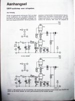
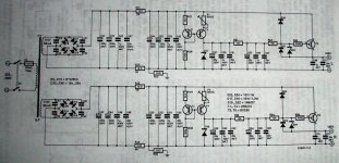
I`m i can add a schematic of a ecc88 tube section for analogue out the TDA1541A?
Don`t be offend if i add info that was add befor or something like that.
Here it is ..from a dutch book from 1992 "elektuur Buizenversterkers"
(note: Buizenversterkers = tubeamplifiers)
Its a SRPP stage with Ecc88 at the pins 5-6 right channel and 5-25 left channel
The page with Dutch tekst:
Current output needs to be very low ohms 20 Ohms R1 R2
With a Bessel filter C1,L2,C2 and R1 De emphases with S1
Most Cd players don`t need it
Psu is very complex for stability and more longlife current for the tubes
6v filament instead of 6,3 hmmm don`t like that course it hurts the dynamics (try to get it on 6,3V is my opinion) AC filament sounds better then DC (not to be applied into Phonostages )
If you need any explanation on this Dutch .... try me or another dutch reader
Hope i did it right to add a tubestage on digital
Back in 1992 there where pcb boards and print layouts .... but nowadays?
Hope you enjoy the input
Attachments
Balanced, high amplitude masterclock with less than 1ps jitter (requires no comparator), SN74AUC1G74 with typical 3.5ps jitter, so total jitter equals approx. 4.5ps for BCK timing.
Hi John,
where do you source crystal oscillator with a low jitter value to achieve 4.5 ps at the output after buffering?
with no comparator the waveform is a sine wave. Is the exact moment of switching so precisely defined like with a squarewave with steep ongoing edge?
do you have any suspition about jitter values of a tent clock?
I currently use a tda1541 in nonos mode with clock injection to a squeezebox. the clock used is a module from guido tent. I am really interested to obtain lowest possible jitter values.
Hi Jean-Charles,
I will answer it as soon as possible. Have been kind of busy over the past months.
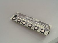
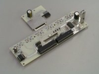
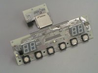
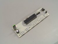
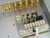
There is a new SD-transport module (MK2) with new improved firmware. Jitter is further reduced by factor 2. There is also a new power supply (MK2) for the SD-player.
I am about to complete a matching stepped shunt volume control unit based on non-inductive wire wound resistors exclusively.
I attached some pictures of these new projects.
You have mail.
I will answer it as soon as possible. Have been kind of busy over the past months.
There is a new SD-transport module (MK2) with new improved firmware. Jitter is further reduced by factor 2. There is also a new power supply (MK2) for the SD-player.
I am about to complete a matching stepped shunt volume control unit based on non-inductive wire wound resistors exclusively.
I attached some pictures of these new projects.
Attachments
Hi dutchaudio,
I don't like Elektuur designs, the fun usually ends as soon the power is applied.
For tube circuits ask the expert:
John Broskie's Guide to Tube Circuit Analysis & Design
I am afraid not.
TDA1541A is rather picky about circuits connected to it. Exceeding TDA1541A output compliance of +25mV and -25mV with respect to GND will increase distortion. In order to minimize on-chip jitter levels at the D/A stage, ripple voltage on the 5V and -15V power supplies need to be minimized. For this reason it is important to direct all used and unused bit currents back into +5V. This means that a passive I/V resistor must connect to +5V rather than GND.
In order to preserve transparency, resolution and low noise (hum) levels, amplification is not desired at all. It is best to generate output signal directly across a passive I/V resistor, 500 Ohm passive I/V resistor will offer 2Vpp without any active amplification. The 500 Ohm impedance is low enough to skip active buffers that would also add substantial distortion.
Digital audio sources produce pulse sequences rather than analogue signals, therefore it is necessary to remove each and every part from the signal path that can introduce distortion (both amplitude and phase). There is no active circuit, no matter how well designed, that can outperform a short piece of wire.
In short, full DC-coupling throughout the audio signal path. If this is not possible, then place the distorting parts at the end of the signal path (speaker crossover).
The issue with TDA1541A output compliance can be fixed using a grounded-gate power MOSFET buffer between TDA1541A output and passive I/V resistor that connects to +5V. DC-coupled output can be obtained by use of an (adjustable) reference voltage that serves as signal reference.
I don't like Elektuur designs, the fun usually ends as soon the power is applied.
For tube circuits ask the expert:
John Broskie's Guide to Tube Circuit Analysis & Design
Hope i did it right to add a tubestage on digital
I am afraid not.
TDA1541A is rather picky about circuits connected to it. Exceeding TDA1541A output compliance of +25mV and -25mV with respect to GND will increase distortion. In order to minimize on-chip jitter levels at the D/A stage, ripple voltage on the 5V and -15V power supplies need to be minimized. For this reason it is important to direct all used and unused bit currents back into +5V. This means that a passive I/V resistor must connect to +5V rather than GND.
In order to preserve transparency, resolution and low noise (hum) levels, amplification is not desired at all. It is best to generate output signal directly across a passive I/V resistor, 500 Ohm passive I/V resistor will offer 2Vpp without any active amplification. The 500 Ohm impedance is low enough to skip active buffers that would also add substantial distortion.
Digital audio sources produce pulse sequences rather than analogue signals, therefore it is necessary to remove each and every part from the signal path that can introduce distortion (both amplitude and phase). There is no active circuit, no matter how well designed, that can outperform a short piece of wire.
In short, full DC-coupling throughout the audio signal path. If this is not possible, then place the distorting parts at the end of the signal path (speaker crossover).
The issue with TDA1541A output compliance can be fixed using a grounded-gate power MOSFET buffer between TDA1541A output and passive I/V resistor that connects to +5V. DC-coupled output can be obtained by use of an (adjustable) reference voltage that serves as signal reference.
- Home
- Source & Line
- Digital Line Level
- Building the ultimate NOS DAC using TDA1541A